Microsoft’s Project Scorpio: More Hardware Details Revealed
This news piece contains speculation, and suggests silicon implementation based on released products and roadmaps. The only elements confirmed for Project Scorpio are the eight x86 cores, 6 TFLOPs, 326 GB/s, it’s built by AMD, and it is coming in 2017. If anyone wants to officially correct any speculation, please get in touch.
One of the critical points of contention with consoles, especially when viewed through the lens of the PC enthusiast, is the hardware specifications. Consoles have long development cycles, and are thus already behind the curve at launch – and that gap only grows over time as the life-cycle of the console is anywhere from five to seven years. The trade-off is usually that the console is an optimized platform, particularly for software: performance is a known quantity and it is much easier to optimize for.
For ten months or so now, Microsoft has been teasing its next generation console. Aside from launching the Xbox One S as a minor mid-season revision to the Xbox One, the next-generation ‘Project Scorpio’ aims to be the most powerful console available. While this is a commendable aspiration (one that would look odd if it wasn’t achieved), the meat and potatoes of the hardware discussion has still been relatively unknown. Well, some of the details have come to the surface through a PR reveal with Eurogamer’s Digital Foundry.
We know the aim with Project Scorpio is to support 4K playback (4K UHD Blu-Ray), as well as a substantial part of 4K gaming. With recent introductions in the PC space of ‘VR’ capable hardware coming down in price, Microsoft is able to carefully navigate what hardware it can source. It is expected that this generation will still rely on AMD’s semi-custom foundry business, given that high-end consoles are now on x86 technologies and Intel’s custom foundry business is still in the process of being enabled (Intel’s custom foundry is also expected to be expensive). Of course, pairing an AMD CPU and AMD GPU would be the sensible choice here, with AMD launching a new GPU architecture last year in Polaris.
Here’s a table of what the reveal is:
| Microsoft Console Specification Comparison | ||||||||||||||
| Xbox 360 | Xbox One | Project Scorpio | ||||||||||||
| CPU Cores/Threads | 3/6 | 8/8 | 8 / ? | |||||||||||
| CPU Frequency | 3.2 GHz | 1.75 GHz | 2.3 GHz | |||||||||||
| CPU µArch | IBM PowerPC | AMD Jaguar | AMD Jaguar | |||||||||||
| Shared L2 Cache | 1MB | 2 x 2MB | 2 x 2MB ? | |||||||||||
| GPU Cores | 16 CUs 768 SPs 853 MHz |
40 CUs 2560 SPs 1172 MHz |
||||||||||||
| Peak Shader Throughput | 0.24 TFLOPS | 1.23 TFLOPS | 6 TFLOPs | |||||||||||
| Embedded Memory | 10MB eDRAM | 32MB eSRAM | None | |||||||||||
| Embedded Memory Bandwidth | 32GB/s | 102-204 GB/s | None | |||||||||||
| System Memory | 512MB GDDR3-1400 | 8GB DDR3-2133 | 12GB GDDR5 (6.8 Gbps) |
|||||||||||
| System Memory Bus | 128-bits | 256-bits | 384-bit | |||||||||||
| System Memory Bandwidth | 22.4 GB/s | 68.3 GB/s | 326 GB/s | |||||||||||
| Manufacturing Process | Various | TSMC 28nm | TSMC 16nm | |||||||||||
At the high level, we have eight ‘custom’ x86 cores running at 2.3 GHz for the CPU, and 40 compute units at 1172 MHz for the GPU. The GPU will be paired with 12GB of GDDR5, to give 326GB/s of bandwidth. Storage is via a 1TB HDD, and the optical drive supports 4K UHD Blu-Ray.
Let’s break this down with some explanation and predictions.
Eight Custom CPU Cores: But They’re Still Jaguar (or almost)
The Xbox One uses AMD’s Jaguar cores. These are low powered and simpler cores, aimed at a low-performance profile and optimized for cost and power. In non-custom designs, we saw these CPUs hit above 2 GHz, but these were limited to 1.75 GHz in the Xbox One.
AMD technically has several cores potentially available for Scorpio: Excavator (Bulldozer-based, as seen on 28nm), Jaguar-based (also from 28nm) or Zen based (seen on 14nm GF). While the latter is a design that has returned AMD to the high-end of x86 performance computing, offering high performance for reasonable power, a Zen design would be relatively quick turnaround from a consumer launch a month ago. Because of the time frame, even if Microsoft could go for Zen in the Scorpio, this would increase the base cost of the console by redesigning the cores on 16nm TSMC.
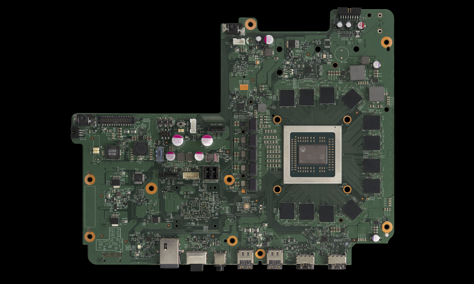
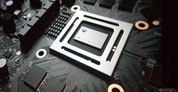
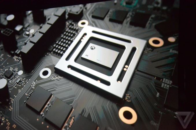
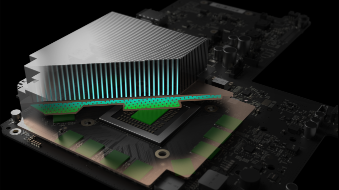
A full shot of the motherboard in Scorpio. Source: Digital Foundry
In the Digital Foundary piece, Microsoft stated that the CPU portion of Scorpio has a 31% performance gain over the Xbox. This isn’t IPC, this is just raw performance. Moving from Jaguar to Zen would be more than 60%, and actually the frequency difference between the 2.3 GHz in Scorpio and 1.75 GHz in Xbox One is exactly 31%. So we are dealing with a Jaguar-style core (although perhaps modified).
That being said, this is a ‘custom’ x86 core. Microsoft could have requested specific IP blocks and features not present in the original Jaguar CPUs but present in things such as Zen, such as power management techniques. Typically a console shares DRAM between the CPU and GPU, so it might be something as simple as the CPU memory controller supporting GDDR5. So instead of seeing Zen coming to consoles, we’re seeing another crack at using Jaguar (or Jaguar+) but revised for a smaller process node to keep overall costs down – and given that the main focus on a console is the GPU, that’s entirely possible.
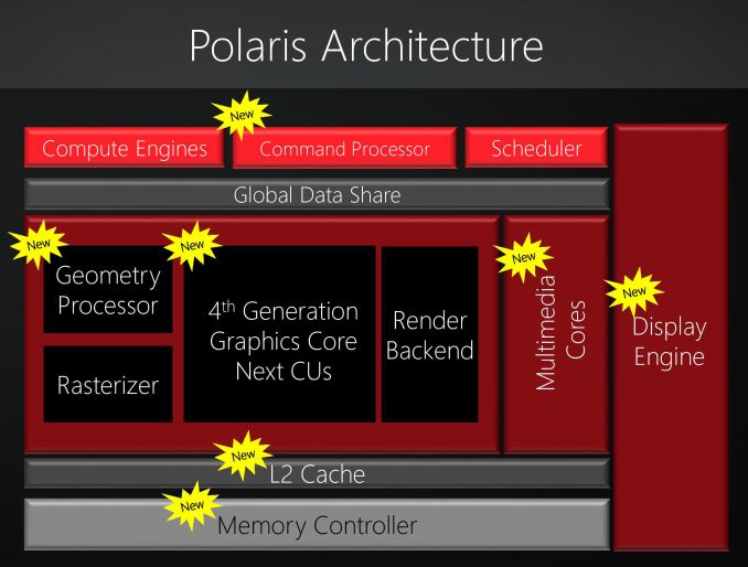
40 Compute Units: Likely Based on AMD’s Polaris GPU Architecture
When it comes to the GPU side of the Scorpio SoC, things get a little more nebulous and interesting. Simply put, we have a pretty good idea that the GPU is based on AMD’s Polaris (GCN4) architecture, but this isn’t something Microsoft is confirming at this time.
While AMD continually moves forward with their GPU architectures every generation, the long development time of the consoles and Microsoft/Sony’s need to customize means that console GPUs can branch off of AMD’s architectures at any number of points. Paradoxically, they can even branch off from future architectures, which is what we saw for the PlayStation 4 Pro last year. There, Sony confirmed that they had used the core shader design from AMD’s forthcoming Vega architecture, which even now has yet to be released on the PC.
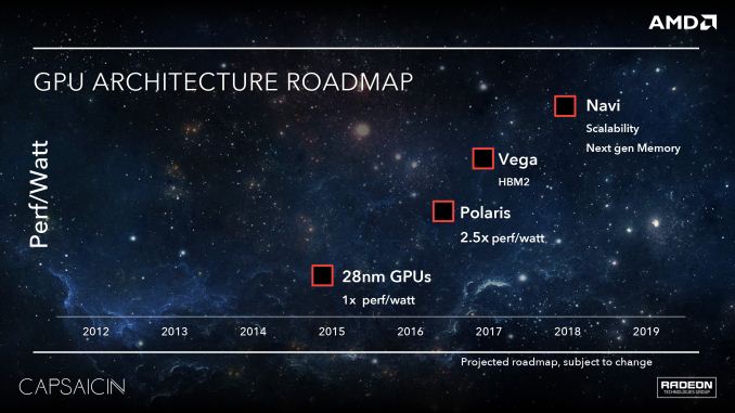
For reference, the original Xbox One and the Xbox One S use a GPU design based on AMD’s GCN 1.1 architecture, roughly equivalent to the Radeon HD 7790. Microsoft’s options for their newest console then are to stick with GCN 1.1, use Polaris (GCN 4), or, like Sony, use something at least in part based on Vega (GCN 5).
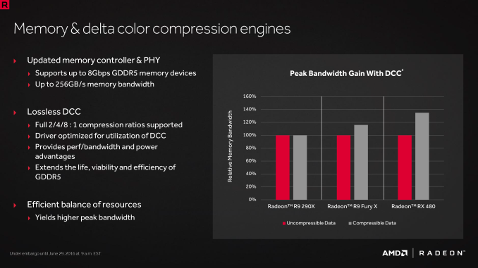
So what did Microsoft use as a base in Scorpio? Right now, based on admittedly limited information from Microsoft’s carefully orchestrated reveal, all signs point to Polaris. Scorpio supports newer features not found in GCN 1.1 such as Delta Color Compression, which is a dead giveaway it’s based on something newer. At the same point, there is no mention in Microsoft’s reveal of any Vega-level features like rapid packed math (2xFP16) or a programmable geometry pipeline. As a result, the safe bet right now is that we’re looking at something principally derived from Polaris.
Now there is a bit of nuance here, as AMD’s GPU architecture is offered piecemeal: the shader cores, the memory controllers, the display controllers, etc are all separate blocks that can be mixed and matches. This is how the PS4 Pro uses just parts of Vega. So it’s entirely possible that there are other bits and pieces in Scorpio that are newer than Polaris, however the all-important shader cores and ROP backends clearly point to Polaris.
Diving into the specs a bit deeper, we do have the clockspeeds and configurations for both the GPU and the memory. Scorpio’s GPU is a 40 CU (2,560 SP) wide design – a bit wider than the Radeon RX 480 – which is a rather extensive upgrade over the original Xbox One. Ignoring clockspeeds for the moment (more in a sec), just the CU count itself is 3.33 times the 12 CUs in the original XB1. Similarly, Microsoft has doubled the number of ROP backends from 16 to 32. The ROP change is badly needed in order for Microsoft to reach their 4K goal, and it has been a pretty universal suspicion that the original XB1’s 16 ROPs were a big part of the reason that major multiplatform games tend to go with 900p instead of a native 1080p.
Meanwhile on the clockspeed front, the new GPU is clocked at 1172MHz, giving Microsoft 6 TFLOPS right on the dot. This is a 37% clockspeed increase over the original XB1, and a 28% increase over the XB1S, which received a slight clockspeed bump of its own. These clockspeeds are well within the range of what the Polaris architecture can offer, and while not as conservative as Sony’s design choices, should still be reasonably power efficient, though I’m very much interested in seeing what total power consumption is like.
More importantly, combined with the much wider GPU, the impact to the various throughput metrics is staggering. Shader/texture throughput will be 4.58x the original XB1, and ROP throughput will be 2.75x. Microsoft had a very large gap to close from the original Xbox One if they wanted to do 4K, and they have certainly put together a design that is equally large to help close that gap. However with that said, with performance that, on paper, is slightly ahead of a Radeon RX 480, I expect we’re still going to see some compromises here to consistently hit Microsoft’s 4K goal. 6 TFLOPS often isn’t enough for native 4K at current image quality levels, which means developers will have to resort to some clever optimizations or image scaling.
Now when it comes to feeding the beast, things take a very interesting turn. Scorpio comes with 12GB of GDDR5 attached to a 384-bit memory bus. This is as opposed to the original Xbox One, which used 8GB of DDR3 on a 256-bit bus, coupled with 32MB of SRAM on the SoC itself. Swapping out the DDR3 + SRAM for GDDR5 makes a lot of sense in the long run, as GDDR5 (as configured on Scorpio) offers 3.2x the bandwidth-per-pin as the DDR3. Microsoft scaled up the GPU, so they needed to scale up its ability to feed it as well.
What makes things especially interesting though is that Microsoft didn’t just switch out DDR3 for GDDR5, but they’re using a wider memory bus as well; expanding it by 50% to 384-bits wide. Not only does this even further expand the console’s memory bandwidth – now to a total of 326GB/sec, or 4.8x the XB1’s DDR3 – but it means we have an odd mismatch between the ROP backends and the memory bus. Briefly, the ROP backends and memory bus are typically balanced 1-to-1 in a GPU, so a single memory controller will feed 1 or two ROP partitions. However in this case, we have a 384-bit bus feeding 32 ROPs, which is not a compatible mapping.
What this means is that at some level, Microsoft is running an additional memory crossbar in the SoC, which would be very similar to what AMD did back in 2012 with the Radeon HD 7970. Because the console SoC needs to split its memory bandwidth between the CPU and the GPU, things aren’t as cut and dry here as they are with discrete GPUs. But, at a high level, what we saw from the 7970 is that the extra bandwidth + crossbar setup did not offer much of a benefit over a straight-connected, lower bandwidth configuration. Accordingly, AMD has never done it again in their dGPUs. So I think it will be very interesting to see if developers can consistently consume more than 218GB/sec or so of bandwidth using the GPU.
Finally, while not touched upon in great deal in Microsoft’s reveal, it’s clear that the GPU portion of Scorpio is otherwise fully modern with respect to its video and display blocks. This doesn’t come as much of a surprise, as it’s necessary to support the 4K UHD Bli-ray standard, and indeed the Xbox One S is already in the same boat. So that means we’re looking at full 4Kp60 HEVC decode with HDMI 2.0 out.
Designing for 16nm at TSMC
If we move forward with a Jaguar plus Polaris prediction, it means that both designs will have to be reconfigured for TSMC’s 16nm process. For the Jaguar-based CPU, it would result in much lower power than 28/32nm, and also a much lower die area. Compared to the GPU, an 8-core Jaguar design might be 10-15% of the entire silicon. The GPU will likely be on similar terms, although with a larger memory bus and more CUs (44 in the design, 40 in use).
AMD recently afforded additional quarterly costs for using foundries other than Global Foundries (as per their renegotiated wafer agreement), which a number of analysts chalked up to future server designs being made elsewhere. A few of us postulated it’s more to do with AMD’s semi-custom business, and either way it points to silicon Zen being redesigned for 16nm TSMC.
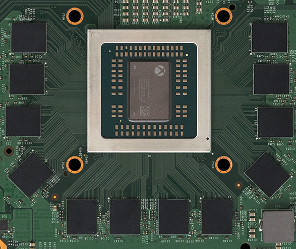
Digital Foundry reported the total die size for the combination chip is listed 360mm2 at seven billion transistors (including CPU and GPU), with four shader engines each containing 11 compute units (one is disabled per block). This is all within 7 billion transistors. It was also mentioned that the floor plan of the silicon, aside from four groups of 11 CUs, also had two clusters of four CPU cores.
Given the use of Jaguar, this means that the CPUs are a tiny chunk of the die area on the silicon, probably under one fifth of the chip. We don’t know the size of the GPU, but 36 CUs of Polaris 10 on GloFo 14nm is 232mm2 at 5.7 billion transistors. Scaled up to 40 CUs, this is around 257 mm2, leaving 100mm2 for the lower density of TSMC’s 16nm process, the CPU cores, a memory controller, and other IO.
Microsoft also states that the power supply with the unit can be suited up to 245W. If we assume a low-frequency Jaguar CPU inside, that could be around 25W max, leaving 150-220W for the GPU. A full sized RX 480 comes in at 150W, and given this GPU is a little more than that, perhaps nearer 170W (or tuned to 100-150W, depending on the base frequencies). The power supply, in a Jaguar + Polaris configuration, seems to have a good 20-25% power budget in hand.
Source: Digital Foundry
Based on some of the discussion from the source, it would seem that AMD is implementing a good number of its power saving features from Excavator and Zen, particularly related to unique DVFS profiles per silicon die as it comes off the production line, rather than a one-size fits all approach. The silicon will also be paired with a vapor chamber cooler, using a custom centrifugal fan.
What We Don’t Know
Hardware aside, the launch titles will be an interesting story in itself, especially with recent closures of dedicated MS studios such as Lionhead.
Project Scorpio is due out in Fall / Q3 2017.
This article originally predicted a Zen + Polaris configuration, but due to a secondary analysis, is now a Jaguar + Polaris prediction.
Source: Digital Foundry