Vulkan Status Update: Will Use Feature Sets, Android Support Incoming
![]()
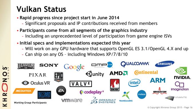
Along with updates on OpenGL, Khronos is also offering a status update on the development of Vulkan at this year’s SIGGRAPH show. Khronos’s next-generation low-level API was announced last year, with further development taking off this year when it was announced at the API would be absorbing Mantle 1.0 and would operate under its current fiery name. The API is still in development, but Khronos has a few new pieces of information to share on the progress of development.
Vulkan Feature Sets
First and foremost, there has been a bit of speculation over how Vulkan would manage being a low-level API for both mobile and desktops, and Khronos is finally answering those questions. In the OpenGL ecosystem, new features would be exposed as optional extensions, and then standardized through core releases (e.g. OpenGL ES 3.2). Due to the factors that resulted in the creation of OpenGL ES, this was never a huge problem for either branch of OpenGL since each could be scoped as appropriate and integrated separately. However with Vulkan there is now just one API, and such a coarse approach would imply limiting Vulkan to just the features mobile GPUs could support, or making even more extensive use of extensions.

To that end, today Khronos is announcing that Vulkan will support defined feature sets in order to help simplify application development and to more readily support mobile and desktop hardware under the same API. Feature sets, as implied by the name, will be groupings of features that will be advertised under a single feature set name, with the idea being that developers will build their programs against a handful of feature sets instead of a massive combination of individual extensions or capability bits (though developers can still use individual features if they’d like). Feature sets are nothing new to desktop graphics, with Microsoft’s DirectX standard having supported them since DirectX 11 in 2009.
While Khronos is announcing that Vulkan will support feature sets, they are not announcing the individual feature sets, and for good reason. In traditional Khronos consortium fashion, Khronos is going to leave the feature set definitions up to the platform holder rather than define those sets themselves. This means that it will typically be the OS developer defining the feature sets, as will be the case on Android. However because Khronos is leaving this up to the platform holder, for holders who opt not to define feature sets for their Vulkan-enabled platforms, Khronos will step in and define those feature sets. In other words platform holders get first dibs, but either way someone will take on the task of defining the feature sets.
Practically speaking, this means that while Android’s feature set will be defined by Google and one can expect SteamOS’s to be defined by Valve, Windows’ feature set will be defined by Khronos. Microsoft is a member of the Khronos consortium and could define it, however Microsoft has taken a hands-off approach on Khronos’s graphics APIs in recent years – presumably in favor of focusing on DirectX – so we’re not expecting to see Microsoft make those definitions. Feature definitions have always been a weak point of the Khronos consortium structure, so giving platform holders the right of first refusal will allow holders such as Google to break the deadlock of the consortium and dictate what features will be supported on Android. Otherwise Khronos will be able to get the job done, though one would expect not without the traditional politics of the consortium.
| Vulkan Feature Set Definitions | |||
| Platform | Expected To Be Defined By | ||
| Android | Platform Holder – Google | ||
| SteamOS | Platform Holder – Valve? | ||
| Linux | Khronos? | ||
| Windows | Khronos (Platform holder Microsoft is anticipated to decline) | ||
Android Support
Speaking of Android, along with announcing their support for OpenGL ES 3.2 today, Google is also announcing that they will be supporting Vulkan in a future release of Android. As with OpenGL ES 3.2, no specific timeline or version of Android is mentioned, though it’s a safe bet that it will be the 2016 release. Android has traditionally heavily relied on OpenGL ES, and with Google sewing further ties with Khronos with the Android Extension Pack, it’s not surprising that Android will include support for Vulkan in order to bring low-level graphics programming to the ecosystem’s developers.

Apple, for what it’s worth, has been absent from the Khronos announcements. As the company is pushing Metal on both mobile and desktop, it looks unlikely that they will be adopting Vulkan any time soon. In which case Vulkan wouldn’t quite match OpenGL ES 3.0’s universal reach due to Apple’s reliance on proprietary APIs.
Vulkan Conformance Tests Will Be Open Source
Meanwhile on the testing and validation front, Khronos is announcing that they are teaming up with Google and the Android Open Source Project to release the Vulkan conformance tests as as open source tests. The tests themselves are being developed by Khronos members and contractors, with the Khronos/ASOP connection coming in to provide the frameworks. The tests themselves are portable to other platforms – Khronos made this point very clear in our briefing – but partnering up with Google helps Khronos get the tests out there sooner and to fulfil their open source goals.

ETA: Late 2015
Finally, Khronos is also offering a bit more guidance on when to expect the first revision of Vulkan. Khronos’s goal for the specification is to release it by the end of the year, which means they should be wrapping up development of the specification soon. Meanwhile driver/runtime development has been occurring concurrently with the development of the specification, which means that the first drivers will be ready at the same time. Khronos does require that there are working implementations before a specification is released to production, so with any luck Vulkan will be ready as a development target and for early end-user testing by the end of 2015.
Update: And speaking of Vulkan’s ETA, there are multiple Vulkan demos on the SIGGRAPH showfloor, demonstrating the API and the current status of vendor implementations. First out of the gate is Imagination, showing off a demo running on Android.