Intel Launches 3D NAND SSDs For Client And Enterprise
Today Intel is announcing a variety of new SSDs with their 3D NAND flash memory. The new models use a mix of 3D MLC and 3D TLC, some SATA and some PCIe, and variously target the consumer, business, embedded and data center markets. While we are still awaiting details on the timing of these product releases, it is clear that Intel is eager to put planar flash behind them. The drive for this is especially strong as the models being replaced are all either based on Intel’s relatively expensive 20nm flash or on 16nm flash that Intel had to buy on the open market due to their decision to not participate in the 16nm node at IMFT.
| Product Series | Market | Interface | 3D NAND |
| SSD 600p | Consumer Client | M.2 PCIe 3 x4 | TLC |
| SSD Pro 6000p | Business Client | M.2 PCIe 3 x4 | TLC |
| SSD E 6000p | Embedded, IoT | M.2 PCIe 3 x4 | TLC |
| SSD E 5420s | Embedded, IoT | 2.5″ and M.2 SATA | MLC |
| SSD DC S3520 | Data Center | 2.5″ and M.2 SATA | MLC |
| SSD DC P3520 | Data Center | U.2 and PCIe x4 HHHL | MLC |
First up, we have a M.2 PCIe SSD branded three different ways for three different markets. In the consumer market we have the SSD 600p series, while the business market will get the Pro 6000p series. The specs released so far differ only in mentioning that the Pro 6000p series will be supported by the remote secure erase feature of Intel’s Active Management Technology. The third variant—for the embedded and Internet of Things market—will only get the two smallest capacities, which gives us a look at how this design will perform with the limited parallelism that results from using IMFT’s high-capacity 384Gb 3D TLC die.
| Intel Client and Embedded PCIe SSDs | |||||
| Model | Pro 6000p | 600p | E 6000p | 750 | |
| Capacity | 128GB, 256GB, 360GB, 512GB, 1024GB | 256GB | 128GB | 400GB, 800GB, 1.2TB | |
| NAND | IMFT 32-layer 3D TLC | IMFT 20nm MLC | |||
| Interface | M.2 2280 PCIe 3 x4 (single-sided) | U.2 or PCIe 3 x4 HHHL | |||
| Sequential Read | up to 1800 MB/s | 1570 MB/s | 770 MB/s | up to 2500 MB/s | |
| Sequential Write | up to 560 MB/s | 540 MB/s | 450 MB/s | up to 1200 MB/s | |
| 4kB Random Read | up to 155k IOPS | 71k IOPS | 35k IOPS | up to 460k IOPS | |
| 4kB Random Write | up to 128k IOPS | 112k IOPS | 91.5k IOPS | up to 290k IOPS | |
| Idle Power | 10mW | 4W | |||
| Warranty | 5 years | 5 years | |||
The 600p and 6000p series are a much more mainstream design than Intel’s previous NVMe SSD for the client market. The SSD 750 was a thinly-disguised enterprise drive, with power consumption and physical dimensions that are far too big for the M.2 form factor that has become the preferred choice for client PCIe storage. The SSD 750 was in many ways overkill from the start, and more recent M.2 drives (especially from Samsung) have caught up in peak performance to offer a much better value for typical client usage. The 600p will be going after the client PCIe storage market from the opposite end: as one of the first TLC PCIe SSDs, its performance specifications don’t set any records but it will be a much more value-oriented product than any of the M.2 PCIe SSDs currently on the market. Intel has confirmed that the 600p and 6000p are using a third-party controller. UPDATE: Allyn Malventano at PC Perspective has uncovered a forum post with an uncensored picture of the 600p. The controller has “SMI” in big letters, suggesting that it is a Silicon Motion SM2260 or relative thereof, but with different markings than the samples Silicon Motion has been showing off at conventions. Intel has also used Silicon Motion controllers in drives like the 540s.

SSD 600p
In addition to the SSD E 6000p, there is a new series of SATA drives for the embedded market. The SSD E 5420s series consists of a 240GB 2.5″ drive and a 150GB M.2 drive, both with 3D MLC and full power loss protection. The E 5420s is rated for one drive write per day, a substantial improvement over the 0.3 DWPD rating of the E 5410s or the 20GB/day of the E 5400s.
| Intel Embedded/IoT SATA SSDs | ||||
| Model | E 5420s | E 5410s | E 5400s | |
| Capacity | 240GB | 150GB | 80GB, 120GB | 48GB, 80GB, 120GB, 180GB |
| NAND | IMFT 32-layer 3D MLC | 16nm MLC | 16nm TLC | |
| Interface | 2.5″ SATA | M.2 SATA | 2.5″ SATA | 2.5″ and M.2 SATA |
| Sequential Read | 320 MB/s | 165 MB/s | up to 475 MB/s | up to 560 MB/s |
| Sequential Write | 300 MB/s | 145 MB/s | up to 135 MB/s | up to 475 MB/s |
| 4kB Random Read | 65k IOPS | 39k IOPS | up to 68k IOPS | up to 71k IOPS |
| 4kB Random Write | 16k IOPS | 28k IOPS | up to 84k IOPS | up to 85k IOPS |
| Warranty | 5 years | 5 years | 5 years | |

SSD E 5420s
Moving on to the data center products, the SSD DC S3520 is a new mid-range enterprise SATA SSD for read-oriented workloads and the third iteration of the S3500 series. The M.2 form factor has returned as an option after the DC S3510 series was only offered in the 2.5″ form factor. As with the SATA drives for the embedded market, performance has decreased but endurance has been bumped up from 0.3 DWPD to 1 DWPD. The larger per-die capacity of the 3D MLC has caused the smallest capacity option to increase from 80GB to 150GB, but 1.6TB is still the largest option for the 2.5″ form factor.
| Intel Enterprise SATA SSDs | |||
| Model | DC S3520 | DC S3510 | |
| Capacity | 150GB, 240GB, 480GB, 800GB, 960GB, 1.2TB, 1.6TB | 150GB, 240GB, 480GB, 760GB, 960GB | 80GB, 120GB, 240GB, 480GB, 800GB, 1.2TB, 1.6TB |
| NAND | IMFT 32-layer 3D MLC | 16nm MLC | |
| Interface | 2.5″ SATA | M.2 SATA | 2.5″ SATA |
| Sequential Read (up to) | 450 MB/s | 410 MB/s | 500 MB/s |
| Sequential Write (up to) | 380 MB/s | 320 MB/s | 460 MB/s |
| 4kB Random Read (up to) | 67.5k IOPS | 53k IOPS | 68k IOPS |
| 4kB Random Write (up to) | 17k IOPS | 14.4k IOPS | 20k IOPS |
| Endurance | 1 DWPD | 1 DWPD | 0.3 DWPD |
| Warranty | 5 years | 5 years | 5 years |

SSD DC S3520
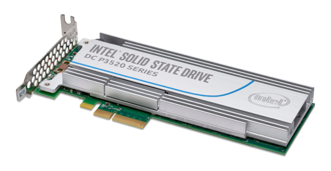
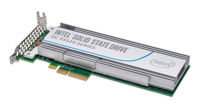
(UPDATED) Finally, for the enterprise PCIe space we have the SSD DC P3520. In March the DC P3320 was announced as Intel’s first 3D NAND SSD and the P3520 was mentioned but specifications were not provided at that time. Intel has since decided to only produce the P3520 and to price it close to the level of SATA SSDs. The reduced performance relative to the DC P3500 is a consequence of reduced parallelism at the same capacity that results from using the 256Gb 3D MLC rather than 128Gb 20nm MLC, and the size of this performance regression is a bit dismaying. The DC P3520 is clearly based on the same hardware platform as the rest of the PCIe data center drives, with a familiar layout for the PCB and heatsink evident in the add-in card version.
| Intel Enterprise PCIe SSDs | |||
| Model | DC P3520 | DC P3320 (canceled) | DC P3500 |
| Capacity | 450GB (U.2 only), 1.2TB, 2TB | 450GB (U.2 only), 1.2TB, 2TB | 400GB, 1.2TB, 2TB |
| NAND | IMFT 32-layer 3D MLC | IMFT 32-layer 3D MLC | IMFT 20nm MLC |
| Interface | U.2 and PCIe 3 x4 HHHL | U.2 and PCIe 3 x4 HHHL | U.2 and PCIe 3 x4 HHHL |
| Sequential Read (up to) | 1700 MB/s | 1600 MB/s | 2700 MB/s |
| Sequential Write (up to) | 1350 MB/s | 1400 MB/s | 1800 MB/s |
| 4kB Random Read (up to) | 375k IOPS | 365k IOPS | 430k IOPS |
| 4kB Random Write (up to) | 26k IOPS | 22k IOPS | 28k IOPS |
| 4kB Random 70/30 Read/Write (up to) | 80k IOPS | 65k IOPS | 80k IOPS |
| Warranty | 5 years | 5 years | 5 years |

SSD DC P3520 U.2
These new SSDs will have a staggered release over the rest of the year. Starting next week the DC P3520 will be shipping, as well as the 128GB, 256GB and 512GB capacities of the SSD 600p and SSD Pro 6000p. The 2.5″ DC S3520 will ship in early September. The rest are planned to be available in Q4.