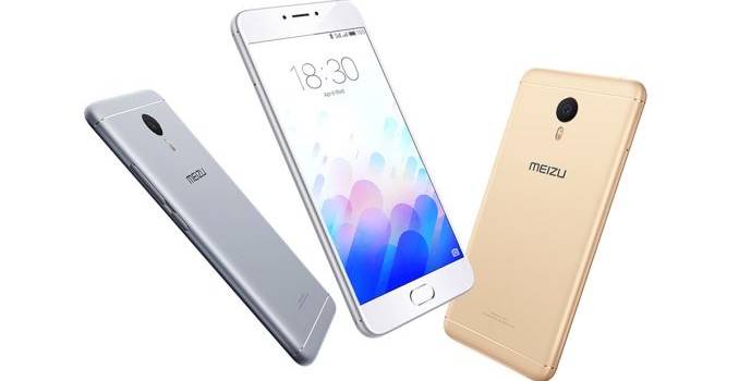
Meizu Launches the m3 note

With every year, we tend to see quite a few launches happen in the first two quarters as the cycles in supply chains align for mass production to start around this time. We’ve already seen a number of new products from Huawei, LG, Samsung, and Xiaomi. Meizu is the latest company to join this list with its announcement of the m3 note.
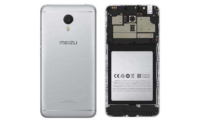
With a 6061 aluminum unibody design, the m3 note draws heavily from the PRO 5. The rear camera is accentuated by a large, black surround with the pill-shaped dual-color LED flash sitting just below. Unlike the PRO 5, however, the camera sits flush with the back. Meizu’s unique T-slot design also carries over from the PRO 5. Instead of the usual plastic antenna strips, Meizu machines slots into the aluminum back, whose polished finish provides a nice contrast to the sandblasted aluminum.
The volume rocker switch sits above the power button inside a groove machined into the right edge, while the SIM and SD card combo slot is on the left edge. A 3.5mm headphone jack is found up top. The downward firing speaker sits next to a centered microUSB port on the bottom.
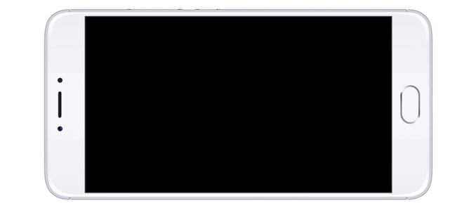
The m3 note’s 5.5-inch FHD IPS display—which reaches a peak brightness of 450 nits, according to Meizu—sits behind edge-to-edge glass. There’s also an mTouch 2.1 fingerprint sensor below the screen that’s surrounded by a stainless steel accent ring. Overall, the rounded corners, beveled edges, and 2.5D curved cover glass give the m3 note a similar in-hand feel to the iPhone 6s Plus.
| Meizu m3 note Specifications | ||
| SoC | MediaTek Helio P10 (MT6755) 4 x 1.8GHz Cortex A53 (Performance) 4 x 1.0GHz Cortex A53 (Efficiency) Mali T860MP2 |
|
| RAM | 2/3GB LPDDR3-833 | |
| NAND | 16/32GB (eMMC 5.1) + microSD | |
| Display | 5.5″ 1920×1080 IPS LCD | |
| Modem | 2G / 3G / 4G LTE Category 6 (Integrated MediaTek WorldMode) Dual SIM DSDS |
|
| Mainland China variant
GSM: B2/B3/B8/B5 |
International Market variant
GSM: B2/B3/B8/B5 WCDMA: B1/B5/B8 TDD-LTE: B40 |
|
| Dimensions | 153.8mm x 75.6mm x 8.2mm; 163g | |
| Camera | Rear Facing 13MP f/2.2 PDAF Dual LED Flash |
|
| Front Facing 5MP f/2.0 |
||
| Battery | 4100 mAh (15.79Wh) | |
| Launch OS | Android 5.1 with Flyme 5.1 UI | |
| Connectivity | 802.11 a/b/g/n/ac, Bluetooth 4.0 GPS/GNSS, Micro USB 2.0, DLNA |
|
| Launch Price (CN) | 799/999 RMB (125/155 USD) 2GB/3GB | |
Inside the aluminum chassis is an octa-core MediaTek Helio P10 SoC. This midrange SoC uses four ARM Cortex-A53 CPUs with a max frequency of 1.8GHz and another four with a max frequency of 1.0GHz in a big.LITTLE arrangement. These frequencies are a little below the P10’s rated frequencies of 2.0GHz and 1.1GHz, respectively. So either Meizu is underclocking the P10 to save power, or it’s using a lower-binned version of the P10.
The P10 SoC also includes an ARM Mali-T860MP2 GPU. This is ARM’s current midrange GPU, which features two ALUs per core instead of three ALUs per core like the high-end Mali-T880.
The m3 note comes in two different configurations: 2GB RAM / 16GB internal storage and 3GB RAM / 32GB internal storage. Both versions support microSD cards for storage expansion and feature a rather large 4100 mAh battery, which should provide the m3 note and its lower-clocked P10 SoC with excellent battery life.
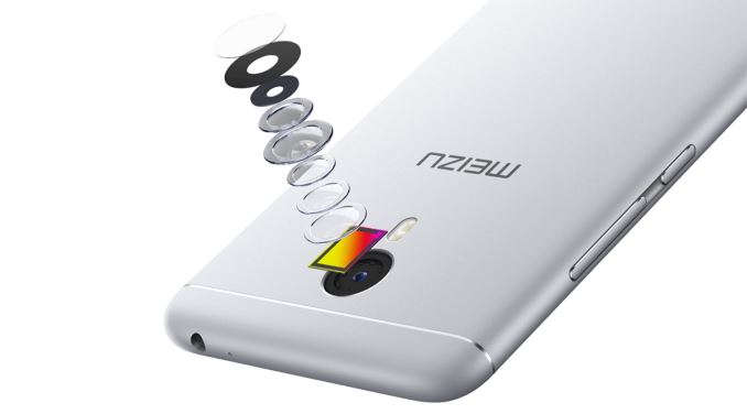
The 13MP rear camera sits behind a 5-piece lens array with an f/2.2 aperture. It’s unclear who makes the sensor, but it does use PDAF to improve focus speed. There’s no OIS support, which is a feature that has yet to trickle down to this price point. The m3 note records video at up to 1080p30, a limit imposed by the P10 SoC.
The m3 note comes in three different colors: gold/white, silver/white, and gray/black. It will be available in China for 799 and 999 RMB for the 2GB and 3GB models respectively. The m3 note will also be available India, Russia, France, Spain, Brazil, Italy, Russia and several other countries throughout Europe, Southeast Asia, Middle East and Latin America, with exact pricing to be determined.