If you follow PC technology news, you would have seen our news on how Supermicro had enabled overclocking for Skylake (Intel’s 6th Generation) processors on non Z170 motherboards. This was a two fold increase in interest – not only was there overclocking (via base frequency rather than multiplier) on an H series chipset more than a few MHz, but it also enabled this type of overclocking on locked processors from $60 and up.

Core i3-6300T overclocked by 20%
We reported at the time that ASRock was also introducing this feature, and since then they promoted a new series of ‘Sky OC’ features to enable base frequency overclocking on locked (often called ‘non-K’ because these chips do not have the K letter in their name to denote overclocking) processors. At CES we were shown new motherboards that were not Z170 motherboards that also had the vital feature – the extra signal generator required for the processor to enable this and a variant of custom firmware. Other motherboard manufacturers were also interested in pursuing this line, although they were a little more reserved.
Since that news we have sourced both the Supermicro motherboard that started the trend as well as more mid-range Core i3 processor for a review. Testing is almost complete, but there is a new climax to this story.
In the past week or so, it turns out that this feature is being removed for non-overclocking focused CPUs. The most obvious indication that this feature is no-longer part of the ecosystem comes from ASRock – their BIOS updates lists new firmware for all of their models which have the feature removed with the following phrase:

The marketing for this feature has all been removed as well, from ASRock’s websites and adverting.
When we (and other media) spoke to the other motherboard manufacturers, noting how reserved they were at the time this ‘feature’ came to prominence; we were told that it was still a work in progress for them. Some were uneasy to guarantee stability, or were not in a position to issue direct updates as some of their products did not have the required hardware and it would have left a confusing product stack with some having the feature and others not. As a result we expected to see new motherboards with the feature over time, either ‘revision/mark 2’ variants or a hold out for the Kaby Lake platform later this year and introduce it there.
Since ASRock were removing the feature, there have been plenty of comments abound on forums as to the reason behind this. The removal of the feature also comes with a CPU microcode update, which is notable because it could mean that both updates are linked. Most are pointing the finger at Intel, wondering if they are flexing some muscle requiring the manufacturer to change the firmware, or it’s being done via microcode, while some are blaming the media for featuring it as a big wow factor and bringing it into the radar more prominently. I want to address some of these points and a wider look at Intel’s strategy here.

Firstly, no matter which way you slice it, Intel has been actively promoting overclocking as a big feature of their processors. It was a big part of the Skylake launch back in August last year.
To put some history in here, overclocking the processor by the the base frequency was common place with Conroe, and then with Nehalem there were special SKUs that opened up the multiplier. With Sandy Bridge, the microarchitecture was designed very differently and more parts of the silicon were integrated into the same clock domain which restricted any base frequency overclocking quite severely. Intel also restricted overclocking via the multiplier to a couple of parts with K in the name (typically high end i5 and i7 parts) such that overclocking could be focused on the high margin processors. This meant that users had to focus on getting more out of the better silicon, rather than pushing a mid-range part into a better performance chip. Some may argue this was to increase high end processor sales, while others saw it as Intel having a performance lead and being able to structure their product stack in such a way to maximize that lead.
In July 2014, with Devil’s Canyon, Intel adjusted the beams slightly. Partly due to an increase in temperature generation with the integrated voltage regulator on Haswell and a decrease in thermal interface quality, Devil’s Canyon was released offering more thermal headroom and potentially better overclocking performance – we tested the i7-4790K and i5-4690K and came to this conclusion. Alongside the two Devil’s Canyon processors they also released an overclockable Pentium processor, the G3258, to mark the 20th anniversary of Pentium. This was a dual core part without hyperthreading which offered a 30-40% overclock, but as we found out in the review of the G3258, even with this OC the fact that it was dual core limited its usefulness in a word were software/gaming is designed to handle more than two threads. At the time, for most enthusiasts, it was clear that if Intel wanted to relaunch the mid-range market, then an unlocked Core i3 needed to be made. It has been clear that while Intel holds the competitive advantage, that was not on the cards – releasing an unlocked Core i3 would give users performance of an i5/i7 at a much lower price point, and would cannibalize sales of their high end parts. While they had no competition for raw CPU horsepower, it wasn’t going to happen, regardless of how heavily Intel was promoting overclocking and how good overclocked processors were for gaming.
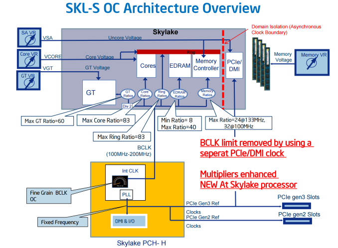
Fast forward to Skylake, and the first processors released were the two overclocked chips – the i7-6600K and i5-6500K, which we reviewed on day one. These were released at Gamescom in August 2015, a primarily gaming focused event and were marketed as unlocked parts ideal for gaming. These processors were arguably as rare as hen’s teeth to find until September. It was more at IDF, a couple of weeks later, that we given that the architectural details of the new CPUs and allowed us to explain why we were seeing the performance numbers we did. The reason why they were released at Gamescom was simply for the gaming crowd, as gaming is one of the few growth markets in the PC industry, but it meant that the overclocking discussions happened later at IDF. Intel invited experienced overclockers on stage during the presentations to show off overclocking on the new parts – it was clear that overclocking is on the agenda. We found out at IDF that the new Skylake microarchitecture uses separate frequency domains for the IO and PCIe, allowing the base frequency of these new unlocked parts to be adjusted as well as the multiplier.

Splave and L0ud_sil3nc3 at IDF 2015 overclocking live with Intel’s Kirk Skaugen (source)

Brian Krzanich, CEO of Intel, with Splave, L0ud_sil3nc3 and Fugger during IDF 2015 (source)
In September 2015, the other members of the Skylake family were released: the 65W parts, the lower power parts, the Core i3 and the Pentium processors. Despite what was being said about being committed to overclocking as a concept/feature, these parts as we expected were locked down in terms of multiplier, but surprisingly locked down in base frequency as well. We had a chance to test some 65W parts, but were only able to move 3% or so, and this was a hard wall rather than a decline.

Core i3-6320 overclocked to 127 MHz on a Supermicro C7H170-M
So again, move forward to November 2015, when we wrote about Supermicro working around this 3% limitation using an external clock generator and modified firmware. It essentially opened the floodgates – not only could you overclock by adjusting the base frequency on a non Z-series chipset, but also on processors that were previously locked or only moved 3%. There was still the limitation of the DRAM increasing in frequency, but it was good enough for enthusiasts to start asking about the motherboard and other motherboard manufacturers to do something similar. Very quickly we were speaking to all the major players about their plans, with ASRock leading the way in that regard. They were quick enough to roll out the new feature on motherboards that could support it, and were taking motherboards already on the design stage up a notch to support it. We tested the i3-6100TE and got to 140 MHz very easily without any voltage increases, giving a 40% overclock.
So in this past week, ASRock has rolled back this feature on the latest BIOS updates. I am in contact with Supermicro as to their perspective on all this. Because of the scale of the rollback and how sudden it was, it is understandable that many users are pointing the finger at Intel, and wondering if there is some muscle being flexed to make this rollback occur. There is obvious finger pointing – if motherboard manufacturers had this feature, and a overclocked Core i3 performed as well as a Core i5-6600K in games, then users might spend $100 less on the processor. Not only end users, but system integrators as well would take advantage of this, offering cheaper pre-overclocked systems that gave higher performance. It would mean that users would upgrade today and keep their system longer, which might be contrary to any strategy for reinvigorating the PC market. Not only the CPU, but saving money on chipsets by buying H or B series would also affect the bottom line.
If you believe that Intel is worth pointing the finger at here, there are plenty of signs that show the two conflicting sides of interest – while promoting overclocking as a major part of the platform on one hand, not allowing overclocking on the low end SKUs with the other seems at odds with the overclocking strategy. There is something to be said about controlling the user experience, making sure the user gets what they paid for rather than a burning pile of rubble due to misconfiguration, or we could look to the fact that if base frequency overclocking is occurring now, then it would invariably end up with Kaby Lake as well. Depending on how Kaby Lake turns out, this might (or might not) be a good (or bad) thing for Intel.
Of course, there could be a few dangers given it was enabled mid-cycle. Allowing overclocking on an H-series or B-series chipset might not be a good thing, especially if the motherboard is only designed for 65W parts from a power delivery perspective. If the CPU is designed for 35W/65W and starts to draw 120W+ or 200W+, with a motherboard that was only expecting 65W, then it would not last very long. That would mean some motherboards would have to be engineered to do so, but as mentioned before, having a blanket upgrade regardless of the motherboard design would leave the company product stack with some parts that could and others that couldn’t, potentially confusing end-users.
Also of potential concern/confusion here are warranty matters for overzealous overclocks. As part of their overclocking strategy Intel does in fact offer overclocking warranties in some regions via their optinal ‘Performance Tuning Protection’ plans, but again this is only for SKUs that are unlocked. With lower-end processors I think it’s safe to say that Intel doesn’t want to open the door again to replacing lower-margin processors that died under “mysterious circumstances” while trying to balance that with legitimate consumer warranty needs.
Arguably the best way to encourage these CPUs to be opened up is some strong competition. It’s at this point that I should add that despite the opening up of the clock domains with Skylake, Intel has been clear in talking about their overclock strategy only in relation to the unlocked parts. This makes sense given their market position.
Back on the motherboard side, assuming that Supermicro will also have to roll back their feature (or limit it to that single motherboard only, which might be difficult to get hold of), then there are two options here for anyone who had invested in the base frequency ecosystem. Either stay on the older BIOS and not update as time goes on, or update and lose the feature. We’re not sure if ASRock will keep the BIOSes that allow base frequency on their website, or if they will be removed so new users cannot roll back the BIOS. I assume that some forums have taken a copy while they were all still available and hosted them elsewhere, such as the overclocking forum HWBot or at XtremeSystems.
Not to mention, there’s the consideration for reviewers as well. For those that have an OC capable system for these locked parts, creating data at an overclocked speed and base speed means double the time to test, although there will be fewer users able to buy the hardware necessary to do so as time goes on. From a personal perspective, I still want to see those OC numbers on Core i3 or Pentiums, or even the Core i5-6400/6500 where a user could have saved $60 compared to the i5-6600K, or comparing that to what the competitors have to offer. How OC makes a difference allows us to predict performance. I assume our readers want to see as well?
Relevant Reading
Devil’s Canyon Review: Core i7-4790K and Core i5-4690K – CPU Review
The Overclockable Pentium G3258 Review – CPU Review
Skylake-K Review: Core i7-6700K and Core i5-6600K – CPU Review
Comparison between the i7-6700K and i7-2600K in Bench – CPU Comparison
Overclocking Performance Mini-Test to 4.8 GHz – Overclocking
Skylake Architecture Analysis – Architecture
Z170 Chipset Analysis and 55+ Motherboards at Launch – Motherboard Overview
Discrete Graphics: An Update for Z170 Motherboards – PCIe Firmware Update