
As has become tradition at CES, the first major press conference of the show belongs to NVIDIA. In previous years their press conference would be dedicated to consumer mobile parts – the Tegra division, in other words – while more recently the company’s conference has shifted to a mix of mobile and automobiles. Finally for 2016, NVIDIA has made a full transition over to cars, with this year’s press conference focusing solely on the subject and skipping consumer mobile entirely.
At CES 2015 NVIDIA announced the DRIVE CX and DRIVE PX systems, with DRIVE CX focusing on cockpit visualization while DRIVE PX was part of a much more ambitious entry into the self-driving vehicle market for NVIDIA. Both systems were based around NVIDIA’s then-new Tegra X1 SoC, implementing it either for its graphics capabilities or its compute capabilities respectively.
For 2016 however, NVIDIA has doubled-down on self-driving vehicles, dedicating the entire press conference to the concept and filling the conference with suitable product announcements. The headline announcement for this year’s conference then is the successor to NVIDIA’s DRIVE PX system, the aptly named DRIVE PX 2.
From a hardware perspective the DRIVE PX 2 is essentially picking up from where the original DRIVE PX left off. NVIDIA continues to believe that the solution to self-driving cars is through computer vision realized by neural networks, with more compute power being necessary to get better performance with greater accuracy. To that while DRIVE PX was something of an early system to prove the concept, then DRIVE PX 2 is NVIDIA is thinking much bigger.
| NVIDIA DRIVE PX Specification Comparison |
| |
DRIVE PX |
DRIVE PX 2 |
| SoCs |
2x Tegra X1 |
2x Tegra “Parker” |
| Discrete GPUs |
N/A |
2x Unknown Pascal |
| CPU Cores |
8x ARM Cortex-A57 +
8x ARM Cortex-53 |
4x NVIDIA Denver +
8x ARM Cortex-A57 |
| GPU Cores |
2x Tegra X1 (Maxwell) |
2x Tegra “Parker” (Pascal) +
2x Unknown Pascal |
| FP32 TFLOPS |
> 1 TFLOPS |
8 TFLOPS |
| FP16 TFLOPS |
> 2 TFLOPS |
16 TFLOPS? |
| TDP |
N/A |
250W |
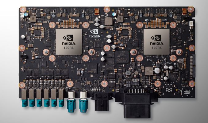
As a result the DRIVE PX 2 is a very powerful – and very power hungry – design meant to offer much greater compute performance than the original DRIVE PX. Based around NVIDIA’s newly disclosed 2016 Tegra (likely to be Parker), the PX 2 incorporates a pair of the SoCs. However in a significant departure from the original PX, the PX 2 also integrates a pair of Pascal discrete GPUs on MXM cards, in order to significantly boost the GPU compute capabilities over what a pair of Tegra processors alone could offer. The end result is that PX 2 packs a total of 4 processors on a single board, essentially combining the two Tegras’ 8 ARM Cortex-A57 and 4 NVIDIA Denver CPU cores with 4 Pascal GPUs.

NVIDIA is not disclosing anything about the discrete Pascal GPUs at this time beyond the architecture and that, like the new Tegra, they’re built on TSMC’s 16nm FinFET process. However looking at the board held up by NVIDIA CEO Jen-Hsun Huang, it appears to be a sizable card with 8 GDDR5 memory packages on the front. My gut instinct is that this may be the Pascal successor to GM206 with the 8 chips forming a 128-bit memory bus in clamshell mode, but at this point that’s speculation on my part.
Update Kudos to our readers on this one. The MXM modules in the picture are almost component-for-component identical to the GTX 980 MXM photo we have on file. So it is likely that these are not Pascal GPUs, and that they’re merely placeholders.
What isn’t in doubt though are the power requirements for PX 2. PX 2 will consume 250W of power – equivalent to today’s GTX 980 Ti and GTX Titan X cards – and will require liquid cooling. NVIDIA’s justification for the design, besides the fact that this much computing power is necessary, is that a liquid cooling system ensures that the PX 2 will receive sufficient cooling in all environmental conditions. More practically though, the company is targeting electric vehicles with this, many of which already use liquid cooling, and as a result are a more natural fit for PX 2’s needs. For all other vehicles the company will also be offering a radiator module to use with the PX 2.

Otherwise NVIDIA never did disclose the requirements for the original PX, but it’s safe to say that PX 2 is significantly higher. It’s particularly telling that in the official photos of the board with the liquid cooling loops installed, it’s the dGPUs we clearly see attached to the loops. Consequently I wouldn’t be surprised if the bulk of that 250W power consumption comes from the dGPUs rather than the Tegra SoCs.
As far as performance goes, NVIDIA spent much of the evening comparing the PX 2 to the GeForce GTX Titan X, and for good reason. The PX 2 is rated for 8 TFLOPS of FP32 performance, which puts PX 2 1 TFLOPS ahead of the 7 TFLOPS Titan X. However while those are raw specifications, it’s important to note that Titan X is 1 GPU whereas PX 2 is 4, which means PX 2 will need to work around multi-GPU scaling issues that aren’t an issue for Titan X.
Curiously, NVIDIA also used the event to introduce a new unit of measurement – the Deep Learning Tera-Op, or DL TOPS – which at 24 is an unusual 3x higher than PX 2’s FP32 performance. Based on everything disclosed by NVIDIA about Pascal so far, we don’t have any reason to believe FP16 performance is more than 2x Pascal’s FP32 performance. So where the extra performance comes from is a mystery at the moment. NVIDIA quoted this and not FP16 FLOPS, so it may include a special case operation (ala the Fused Multiply-Add), or even including the performance of the Denver CPU cores.
On that note, while DRIVE PX 2 was the focus of NVIDIA’s presentation, it was GTX Titan X that was actually driving all of the real-time presentations. As far as I know we did not actually see any demos being powered by PX 2, and it’s unclear whether PX 2 is even ready for controlled demonstration at this time. NVIDIA mentions in their press release that the PX 2 will be available to early access partners in Q2, with general availability not occurring until Q4.
Meanwhile along with the PX 2 hardware, NVIDIA also used their conference to reiterate their plans for self-driving cars, and where their hardware and software will fit into this. NVIDIA is still aiming to develop a hardware ecosystem for the automotive industry rather than an end-to-end solution. Which is to say that they want to provide the hardware, while letting their customers develop the software.

However at the same time, in an action admitting that it’s not always easy for customers to get started from scratch, NVIDIA will also be developing their complete reference platform combining hardware and software. The reference platform includes not just the hardware for self-driving cards – including the PX 2 system and other NVIDIA hardware to train the neural nets – but also software components including the company’s existing DriveWorks SDK, and a pre-trained driving neural net the company is calling DRIVENet.
Consequently while the company isn’t strictly in the process of developing its own cars, it is essentially in the process of training them. Which means NVIDIA has been sending cars around the Sunnyvale area to record interactions, training the 37 million neuron network how to understand traffic. A significant portion of NVIDIA’s presentation was taken up demonstrating DRIVENet in action, showcasing how well it understood the world using a combination of LIDAR and computer vision, with a GTX Titan X running the network at about 50fps. Ultimately I think it’s fair to say that NVIDIA would rather their customers be doing this, building nets on top of systems like DIGITS, but they also have seen first-hand in previous endeavors that bootstrapping an ecosystem like they desire requires having all of the components already there.
Finally, NVIDIA also announced that they have lined up their first customer for PX 2: Volvo. In 2017 the company will be outfitting 100 XC90 SUVs with the PX 2, for use in their ongoing self-driving car development efforts.


