News


Qualcomm Snapdragon 820 Experience: HMP Kryo and Demos

Qualcomm Snapdragon 820 Experience: HMP Kryo and Demos

While the Snapdragon 820 has had a number of announcements about various aspects of the SoC, some details have been mostly left to the imagination. Today, Qualcomm held an event to release some details about Snapdragon 820, but also to show off what can be enabled by Snapdragon 820. Some of the main details released today include some estimates of power, and some additional disclosure on the Kryo CPU cores in Snapdragon 820.

In power, Qualcomm published a slide showing average power consumption using their own internal model for determining days of use. In their testing, it shows that Snapdragon 820 uses 30% less power for the same time of use. Of course, this needs to be taken with appropriate skepticism, but given the use of 14LPP it probably shouldn’t be a surprise that Snapdragon 820 improves significantly over past devices.

The other disclosures of note were primarily centered on the CPU and modem. On the modem side, Qualcomm is claiming 15% improvement in power efficiency which should eliminate any remaining gap between LTE and WiFi battery life.

On the CPU side, while the claims of either doubled performance or power efficiency have been discussed before, new details on the CPU include that the quad core CPU is best described as an HMP solution with two high-performance cores clocked at 2.2 GHz and two low-power cores clocked at 1.6 or 1.7GHz when looking at previous Qualcomm SoCs with two clusters that share an architecture. Qualcomm also disclosed that the CPU architectures of both clusters are identical, but with differences in cache configuration. However, the differences in cache configuration weren’t disclosed. I wasn’t able to get an answer regarding whether this is an ARM big.LITTLE design that uses CCI-400 or CCI-500, but given that there’s an L3 cache shared between clusters it’s more likely that this is a completely custom HMP architecture.

In addition to these disclosures, we saw a number of demos. Probably the single most interesting demo shown was Sense ID, in which it was shown that fingerprint sensing worked properly through a sheet of glass and aluminum. To my recollection both the glass and aluminum were 0.4mm thick, so the system seems to be relatively robust. For those unfamiliar with Sense ID, rather than relying of high-resolution capacitive touch sensing the system uses ultrasonic sound waves to map the fingerprint, which allows it to penetrate materials like glass and metal and improves sensitivity despite contaminants like water and dirt.

One area of note was that Qualcomm is now offering their own speaker amp/protection IC that would compete with ICs like the NXP TFA9895 that are quite common in devices today. The WSA8815 chip would also be able to deliver stereo sound effects in devices with stereo front-facing speakers. It seems that the primary advantage of this solution is cost when bundled with the SoC, but it remains to be seen whether OEM adoption would be widespread.

One of the other demos was improved low light video and photos by using the Hexagon 680 DSP and Spectra 14-bit dual ISP. The main area of interest in this demo was improved visibility of underexposed areas by boosting shadow visibility, while also eliminating the resulting noise through temporal noise reduction.

On the RF side, in addition to showing that the Snapdragon 820 modem is capable of UE Category 12/13 LTE speeds Qualcomm also demonstrated that the Snapdragon 820 is capable of dynamically detecting WiFi signal quality based upon throughput and other metrics that affect VOIP quality and seamlessly handing off calls from WiFi to LTE and back. We also saw a demo for Qualcomm’s closed-loop antenna tuning system which allows for reduced impedance mismatch relative to previous open-loop antenna tuners which loaded various antenna profiles based upon things like touch sensing of certain critical areas.

Qualcomm Snapdragon 820 Experience: HMP Kryo and Demos

Qualcomm Snapdragon 820 Experience: HMP Kryo and Demos

While the Snapdragon 820 has had a number of announcements about various aspects of the SoC, some details have been mostly left to the imagination. Today, Qualcomm held an event to release some details about Snapdragon 820, but also to show off what can be enabled by Snapdragon 820. Some of the main details released today include some estimates of power, and some additional disclosure on the Kryo CPU cores in Snapdragon 820.

In power, Qualcomm published a slide showing average power consumption using their own internal model for determining days of use. In their testing, it shows that Snapdragon 820 uses 30% less power for the same time of use. Of course, this needs to be taken with appropriate skepticism, but given the use of 14LPP it probably shouldn’t be a surprise that Snapdragon 820 improves significantly over past devices.

The other disclosures of note were primarily centered on the CPU and modem. On the modem side, Qualcomm is claiming 15% improvement in power efficiency which should eliminate any remaining gap between LTE and WiFi battery life.

On the CPU side, while the claims of either doubled performance or power efficiency have been discussed before, new details on the CPU include that the quad core CPU is best described as an HMP solution with two high-performance cores clocked at 2.2 GHz and two low-power cores clocked at 1.6 or 1.7GHz when looking at previous Qualcomm SoCs with two clusters that share an architecture. Qualcomm also disclosed that the CPU architectures of both clusters are identical, but with differences in cache configuration. However, the differences in cache configuration weren’t disclosed. I wasn’t able to get an answer regarding whether this is an ARM big.LITTLE design that uses CCI-400 or CCI-500, but given that there’s an L3 cache shared between clusters it’s more likely that this is a completely custom HMP architecture.

In addition to these disclosures, we saw a number of demos. Probably the single most interesting demo shown was Sense ID, in which it was shown that fingerprint sensing worked properly through a sheet of glass and aluminum. To my recollection both the glass and aluminum were 0.4mm thick, so the system seems to be relatively robust. For those unfamiliar with Sense ID, rather than relying of high-resolution capacitive touch sensing the system uses ultrasonic sound waves to map the fingerprint, which allows it to penetrate materials like glass and metal and improves sensitivity despite contaminants like water and dirt.

One area of note was that Qualcomm is now offering their own speaker amp/protection IC that would compete with ICs like the NXP TFA9895 that are quite common in devices today. The WSA8815 chip would also be able to deliver stereo sound effects in devices with stereo front-facing speakers. It seems that the primary advantage of this solution is cost when bundled with the SoC, but it remains to be seen whether OEM adoption would be widespread.

One of the other demos was improved low light video and photos by using the Hexagon 680 DSP and Spectra 14-bit dual ISP. The main area of interest in this demo was improved visibility of underexposed areas by boosting shadow visibility, while also eliminating the resulting noise through temporal noise reduction.

On the RF side, in addition to showing that the Snapdragon 820 modem is capable of UE Category 12/13 LTE speeds Qualcomm also demonstrated that the Snapdragon 820 is capable of dynamically detecting WiFi signal quality based upon throughput and other metrics that affect VOIP quality and seamlessly handing off calls from WiFi to LTE and back. We also saw a demo for Qualcomm’s closed-loop antenna tuning system which allows for reduced impedance mismatch relative to previous open-loop antenna tuners which loaded various antenna profiles based upon things like touch sensing of certain critical areas.

ARM Announces New Cortex-A35 CPU - Ultra-High Efficiency For Wearables & More

ARM Announces New Cortex-A35 CPU – Ultra-High Efficiency For Wearables & More

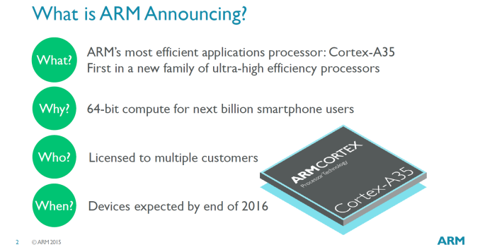
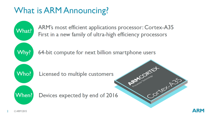
Today as part of the volley of announcements at ARM’s TechCon conference we discover ARM’s new low-power application-tier CPU architecture, the Cortex-A35. ARM follows an interesting product model: The company chooses to segment its IP offerings into different use-cases depending on market needs, designing different highly optimized architectures depending on the target performance and power requirements. As such, we see the Cortex-A lineup of application processors categorized in three groups: High performance, high efficiency, and ultra-high efficiency designs. In the first group we of course find ARM’s big cores such as the Cortex A57 or A72, followed by the A53 in more efficiency targeted use-cases or in tandem with big cores in big.LITTLE designs.

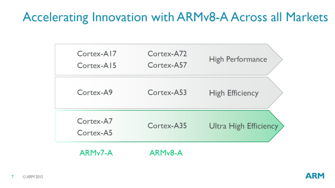
What seems to be counter-intuitive is that ARM sees the A35 not as a successor to the A53, but rather a replacement for the A7 and A5. During our in-depth analysis of the Cortex A53 in our Exynos 5433 review earlier this year I claimed that the A53 seemed to be more like an extension to the perf/W curve of the Cortex A7 instead of it being a part within the same power levels, and now with the A35 ARM seems to have validated this notion.

As such, the A35 is targeted at power targets below ~125mW where the Cortex A7 and A5 are still very commonly used. To give us an idea of what to expect from actual silicon, ARM shared with us a figure of 90mW at 1GHz on a 28nm manufacturing process. Of course the A35 will see a wide range of implementations on different process nodes such as for example 14/16nm or at much higher clock rates above 2GHz, similar to how we’ve come to see a wide range of process and frequency targets for the A53 today.

Most importantly, the A35 now completes ARM’s ARMv8 processor portfolio with designs covering the full range of power and efficiency targets. The A35 can also be used in conjunction with A72/A57/A53 cores in big.LITTLE systems, enabling for some very exotic configurations (A true tri-cluster comes to mind) depending if vendors see justification in implementing such SoCs.

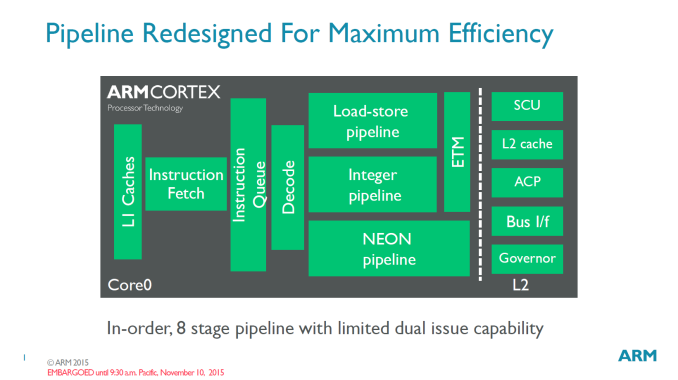
At heart, the A35 is still an in-order limited dual-issue architecture much like the A7 or A53. The 8-stage pipeline depth also hasn’t changed so from this high-level perspective we don’t see much difference in comparison to preceding designs. What ARM has done though is to improve the individual blocks for better performance and efficiency by having bits and pieces of architectural enhancements that are even newer than what big cores such as the A72 currently employ.
 
Areas where the A35 had focused attention on are front-end efficiency improvements, such as a redesigned instruction fetch unit that improves branch prediction. The instruction fetch bandwidth was balanced for power efficiency while the instruction queue is now smaller and also tuned for efficiency
 
It’s especially on memory benchmarks where the A35 will shine compared to the A7: The A35 adopts a lot of the Cortex A53’s memory architecture. On the L1 memory system of which A35 can have configurable 8 to 64KB of instruction and data caches we now see use of multi-stream automatic data prefetching and automatic write stream detection. The L2 memory system (configurable from 128KB to 1MB) has seen increased buffering capacity and resource sharing while improving write stream efficiency and introducting coherency optimizations to reduce contention.
 
The NEON/FP pipeline has seen the biggest advancements, besides improved store performance the new units now add fully pipelined double precision multiply capability. The pipeline has also seen improvements in terms of area efficiency, part of the reason enabling the A35 to be smaller than the A53.
 
In terms of power management, the A35 much like the A53 now implements hardware retention states for both the main CPU core and NEON pipeline (separate power domains). What seems to be interesting here is that there is now a hardware governor within the CPU cluster able to arbitrate automatic entry and exit for retention states. Until now we’ve seen very little to no use of retention states by vendors, the only SoC that I’ve confirmed to use it was the Snapdragon 810 and that was subsequently disabled in later software updates in favour of just using the core power collapse CPU idle state.

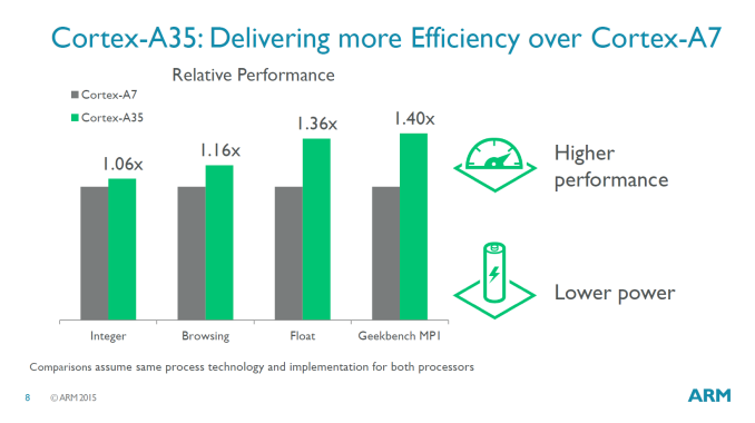
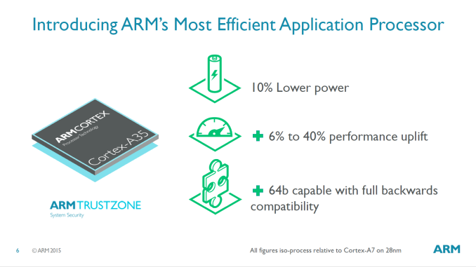
At the same frequency and process, the A35 architecture (codenamed Mercury), promises to be 10% lower power than the A7 while giving an 6-40% performance uplift depending on use-case. In integer workloads (SPECint2006) the A35 gives about 6% higher throughput than the A7, while floating point (SPECfp2000) is supposed to give a more substantial 36% increase.

What is probably more interesting are apples-to-apples performance and power comparisons to the A53. Here the A35 actually is extremely intriguing as it is able to match the A53’s performance from 80% to up to 100% depending on use-case. Browser workloads are where the A35 will trail behind the most and only be able to provide around 80% of the A53’s performance. Integer workloads are quoted at coming in at 84-85% of the Apollo core, while as mentioned earlier, memory-heavy workloads are supposed to be on par with the larger bretheren.

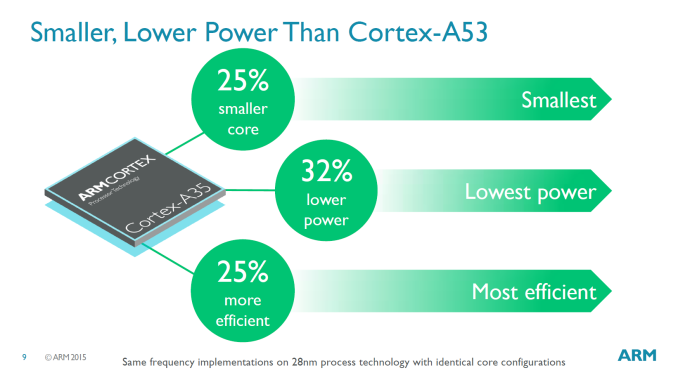
What puts things in perspective though is that the A35 is able to achieve all of this at 75% the core size and 68% the power of the A53. ARM claims that the A35 and A53 may still be used side-by-side and even envisions big.LITTLE A53.A35 designs, but I have a hard time justifying continued usage of the A53 because of the cost incentive for vendors to migrate over to the A35. Even in big.LITTLE with A72 big cores I find it somewhat hard to see why a vendor would choose to continue to use an A53 little cluster while they could theoretically just use a higher clocked A35 to compensate for the performance deficit. Even in the worst-case scenario where the power advantage would be eliminated by running a higher frequency, vendors would still be able to gain from the switch due to the smaller core and subsequent reduced die size.

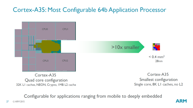
The A35 is touted as ARM’s most configurable processor with vendors able to alter their designs far beyond simple choices such the core-count within a cluster. Designers will now also be able to choose whether they want NEON, Crypto, ACP or even the L2 blocks included in their implementations. The company envisions this to be processor for the next billion smartphone users and we’ll likely see it in a very large variety of SoCs powering IoT devices such as wearables and embedded platforms, to budget smartphones and even high-end ones in big.LITTLE configurations.

ARM expects first devices with the A35 to ship by the end of 2016. Due to the sheer number of possible applications and expected volume, the Cortex A35 will undoubtedly be a very important CPU core for ARM that will be with us for quite some time to come.