Vik


AMD Jumps Into the SSD Market: Radeon R7 Series SSD Launched

AMD Jumps Into the SSD Market: Radeon R7 Series SSD Launched

Back in 2011, AMD made a rather unexpected move and expanded its Radeon brand to include memory in addition to graphics cards. With today’s announcement AMD is adding another member to its Radeon family by releasing Radeon R7 Series SSDs. Similar to AMD memory, AMD is not actually designing or manufacturing the SSDs as the product design and manufacturing is handled by OCZ. In fact, all the customer support is also handled by OCZ, so aside from the AMD logo AMD is not really involved in the product.

Partnering with OCZ makes sense because OCZ’s focus with the Barefoot 3 platform has always been gamers and enthusiasts and that is the target group for AMD’s R7 SSDs as well. OCZ is a now owned by Toshiba, so OCZ has direct access to NAND with guaranteed supply, whereas fabless OEMs (e.g. Kingston) could face supply issues that might harm AMD. Here’s the quick overview, which of course will be essentially the same as certain existing Barefoot 3 products.

AMD Radeon R7 Series SSD Specifications
Capacity 120GB 240GB 480GB
Controller OCZ Barefoot 3 M00
NAND Toshiba A19nm MLC
Sequential Read 550MB/s 550MB/s 550MB/s
Sequential Write 470MB/s 530MB/s 530MB/s
4KB Random Read 85K IOPS 95K IOPS 100K IOPS
4KB Random Write 90K IOPS 90K IOPS 90K IOPS
Steady-State 4KB Random Write 12K IOPS 20K IOPS 23K IOPS
Idle Power 0.6W 0.6W 0.6W
Max Power 2.7W 2.7W 2.7W
Encryption AES-256
Endurance 30GB/day for 4 years
Warranty Four years
MSRP $100 $164 $299

The R7 is based on OCZ’s own Barefoot 3 controller and it is the same higher clocked M00 version (397MHz) as in the Vector 150. The new ARC 100 and Vertex 460 use the M10 version, which runs at 352MHz instead of 397MHz but is otherwise the same silicon. Performance wise the R7 SSD is very close to Vector 150 with slightly lower random write performance, although random read performance is marginally better in turn.

The biggest difference between the two is endurance as the Vector 150 is rated at 50GB per day for five years (91TB total) while the R7 is rated at 30GB per day for four years (43TB total). The firmware in the R7 is tailored for AMD, although I was told that the customizations are mainly wear-leveling related to increase endurance over the Vertex 460, so there should not be any surprises in performance. The NAND is also different as the R7 utilizes Toshiba’s A19nm MLC, but OCZ should be making the switch to A19nm across its whole client SSD lineup soon to cut costs. 

The motivation behind AMD’s move is identical to the reason AMD entered the memory market. AMD wants to provide users an “AMD-only” experience by offering as many of the components as possible. Another argument AMD had is that providing more AMD branded products makes it easier for novice PC builders to pick the parts because the buyer does not have to go through the trouble of deciding between dozens of products and making sure the parts are compatible with each other. In addition to providing an easier purchase experience, AMD can also use the R7 SSDs in bundles and promotions, which is definitely more lucrative than using third party components. 

Of course, the ultimate reason behind the move is that SSDs are becoming a mainstream product, and they provide another revenue source for AMD. AMD has not been doing that great financially lately and having an extra low risk revenue source is definitely welcome, even though client SSDs are not exactly a high profit market anymore. Then again, AMD is not investing much into SSDs since development and manufacturing is done by OCZ, so even if Radeon R7 SSD sales end up being low, AMD has no long-term investment to protect. The announced pricing is generally in line with what we’re seeing for the existing OCZ Vector 150 products, though mail-in rebates can actually drop the Vector 150 below Radeon R7 SSD levels.

All in all, the R7 will not provide much from a technological standpoint since it uses the same platform we have tested several times, but it will be interesting to see how AMD bundles the R7 with other AMD products. AMD now has an opportunity to provide even more extensive bundles (CPU/APU, GPU, RAM and SSD); all that’s left is for AMD to begin offering Radeon branded motherboards, power supplies, and cases to provide the ultimate AMD-only experience. Whether that happens remains to be seen, but AMD is trying an aggressive bundling strategy to increase their desktop CPU sales.

We have samples of the Radeon R7 SSD on the way, so stay tuned for the full review!

AMD Jumps Into the SSD Market: Radeon R7 Series SSD Launched

AMD Jumps Into the SSD Market: Radeon R7 Series SSD Launched

Back in 2011, AMD made a rather unexpected move and expanded its Radeon brand to include memory in addition to graphics cards. With today’s announcement AMD is adding another member to its Radeon family by releasing Radeon R7 Series SSDs. Similar to AMD memory, AMD is not actually designing or manufacturing the SSDs as the product design and manufacturing is handled by OCZ. In fact, all the customer support is also handled by OCZ, so aside from the AMD logo AMD is not really involved in the product.

Partnering with OCZ makes sense because OCZ’s focus with the Barefoot 3 platform has always been gamers and enthusiasts and that is the target group for AMD’s R7 SSDs as well. OCZ is a now owned by Toshiba, so OCZ has direct access to NAND with guaranteed supply, whereas fabless OEMs (e.g. Kingston) could face supply issues that might harm AMD. Here’s the quick overview, which of course will be essentially the same as certain existing Barefoot 3 products.

AMD Radeon R7 Series SSD Specifications
Capacity 120GB 240GB 480GB
Controller OCZ Barefoot 3 M00
NAND Toshiba A19nm MLC
Sequential Read 550MB/s 550MB/s 550MB/s
Sequential Write 470MB/s 530MB/s 530MB/s
4KB Random Read 85K IOPS 95K IOPS 100K IOPS
4KB Random Write 90K IOPS 90K IOPS 90K IOPS
Steady-State 4KB Random Write 12K IOPS 20K IOPS 23K IOPS
Idle Power 0.6W 0.6W 0.6W
Max Power 2.7W 2.7W 2.7W
Encryption AES-256
Endurance 30GB/day for 4 years
Warranty Four years
MSRP $100 $164 $299

The R7 is based on OCZ’s own Barefoot 3 controller and it is the same higher clocked M00 version (397MHz) as in the Vector 150. The new ARC 100 and Vertex 460 use the M10 version, which runs at 352MHz instead of 397MHz but is otherwise the same silicon. Performance wise the R7 SSD is very close to Vector 150 with slightly lower random write performance, although random read performance is marginally better in turn.

The biggest difference between the two is endurance as the Vector 150 is rated at 50GB per day for five years (91TB total) while the R7 is rated at 30GB per day for four years (43TB total). The firmware in the R7 is tailored for AMD, although I was told that the customizations are mainly wear-leveling related to increase endurance over the Vertex 460, so there should not be any surprises in performance. The NAND is also different as the R7 utilizes Toshiba’s A19nm MLC, but OCZ should be making the switch to A19nm across its whole client SSD lineup soon to cut costs. 

The motivation behind AMD’s move is identical to the reason AMD entered the memory market. AMD wants to provide users an “AMD-only” experience by offering as many of the components as possible. Another argument AMD had is that providing more AMD branded products makes it easier for novice PC builders to pick the parts because the buyer does not have to go through the trouble of deciding between dozens of products and making sure the parts are compatible with each other. In addition to providing an easier purchase experience, AMD can also use the R7 SSDs in bundles and promotions, which is definitely more lucrative than using third party components. 

Of course, the ultimate reason behind the move is that SSDs are becoming a mainstream product, and they provide another revenue source for AMD. AMD has not been doing that great financially lately and having an extra low risk revenue source is definitely welcome, even though client SSDs are not exactly a high profit market anymore. Then again, AMD is not investing much into SSDs since development and manufacturing is done by OCZ, so even if Radeon R7 SSD sales end up being low, AMD has no long-term investment to protect. The announced pricing is generally in line with what we’re seeing for the existing OCZ Vector 150 products, though mail-in rebates can actually drop the Vector 150 below Radeon R7 SSD levels.

All in all, the R7 will not provide much from a technological standpoint since it uses the same platform we have tested several times, but it will be interesting to see how AMD bundles the R7 with other AMD products. AMD now has an opportunity to provide even more extensive bundles (CPU/APU, GPU, RAM and SSD); all that’s left is for AMD to begin offering Radeon branded motherboards, power supplies, and cases to provide the ultimate AMD-only experience. Whether that happens remains to be seen, but AMD is trying an aggressive bundling strategy to increase their desktop CPU sales.

We have samples of the Radeon R7 SSD on the way, so stay tuned for the full review!

ARM's Cortex M: Even Smaller and Lower Power CPU Cores

ARM’s Cortex M: Even Smaller and Lower Power CPU Cores

ARM (and its partners) were arguably one of the major causes of the present day smartphone revolution. While AMD and Intel focused on using Moore’s Law to drive higher and higher performing CPUs, ARM and its partners used the same physics to drive integration and lower power. The result was ultimately the ARM11 and Cortex A-series CPU cores that began the revolution and continue to power many smartphones today. With hopes of history repeating itself, ARM is just as focused on building an even smaller, even lower power family of CPU cores under the Cortex M brand.

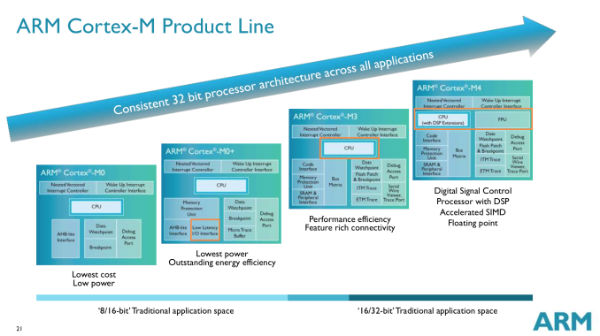
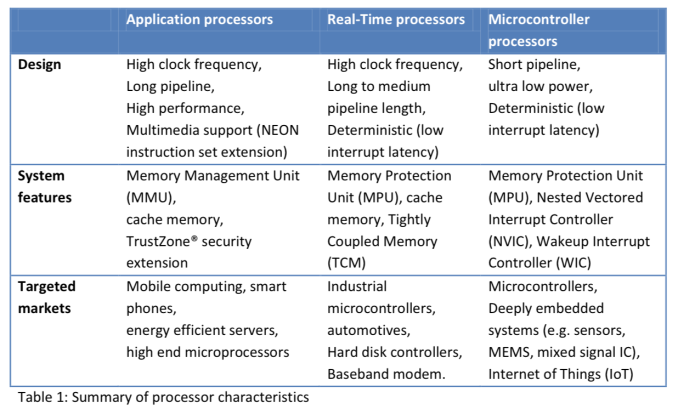
We’ve talked about ARM’s three major families of CPU cores before: Cortex A (applications processors), Cortex R (real-time processors) and Cortex M (embedded/microcontrollers). Although Cortex A is what we mostly talk about, Cortex M is becoming increasingly important as compute is added to more types of devices.

Wearables are an obvious fit for Cortex M, yet the initial launch of Android Wear devices bucked the trend and implemented Cortex A based SoCs. A big part of that is likely due to the fact that the initial market for an Android Wear device is limited, and thus a custom designed SoC is tough to justify from a financial standpoint (not to mention the hardware requirements of running Android outpace what a Cortex M can offer). Looking a bit earlier in wearable history and you’ll find a good number of Cortex M based designs including the FitBit Force and the Pebble Steel. I figured it’s time to put the Cortex M’s architecture, performance and die area in perspective.

We’re very much in the early days of the evolution of Cortex M. The family itself has five very small members: M0, M0+, M1, M3 and M4. For the purposes of this article we’ll be focusing on everything but Cortex M1. The M1 is quite similar to the M0 but focuses more on FPGA designs.

Before we get too far down the architecture rabbit hole it’s important to provide some perspective. At a tech day earlier this year, ARM presented this data showing Cortex M die area:

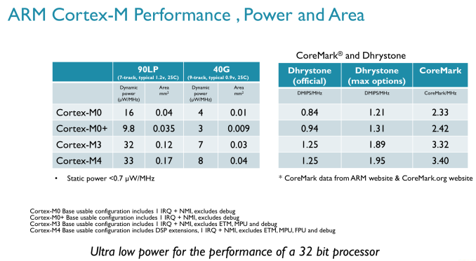
By comparison, a 40nm Cortex A9 core would be roughly around 2.5mm^2 range or a single core. ARM originally claimed the Cortex A7 would be around 1/3 – 1/2 of the area of a Cortex A8, and the Cortex A9 is roughly equivalent to the Cortex A8 in terms of die area, putting a Cortex A7 at 0.83mm^2 – 1.25mm^2. In any case, with Cortex M we’re talking about an order of magnitude smaller CPU core sizes.

The Cortex M0 in particular is small enough that SoC designers may end up sprinkling in multiple M0 cores in case they need the functionality later on. With the Cortex M0+ we’re talking about less than a hundredth of a square millimeter in die area, even the tightest budgets can afford a few of these cores.

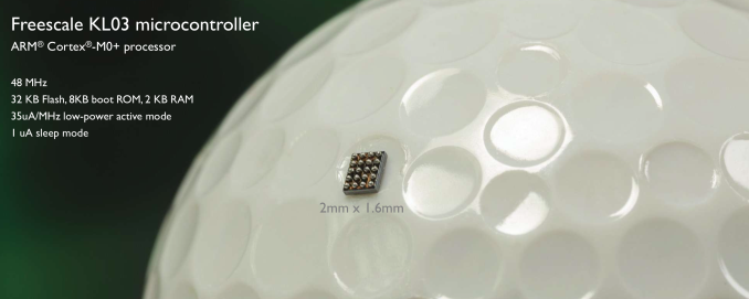
In fact, entire SoCs based on Cortex M CPU cores can be the size of a single Cortex A core. ARM provided this shot of a Freescale Cortex M0+ design in the dimple of a golf ball:

ARM wouldn’t provide me with comparative power metrics for Cortex M vs. Cortex A series parts, but we do have a general idea about performance:

Estimated Core Performance
  ARM Cortex M0/M0+ ARM Cortex M3/M4 ARM11 ARM Cortex A7 ARM Cortex A9 Qualcomm Krait 200
DMIPS/MHz 0.84/0.94 1.25 1.25 1.9 2.5 3.3

In terms of DMIPS/MHz, Cortex M parts can actually approach some pretty decent numbers. A Cortex M4 can offer similar DMIPS/MHz to an ARM11 (an admittedly poor indicator of overall performance). The real performance differences come into play when you look at shipping frequencies, as well as the type of memory interface built around the CPU. Cortex M designs tend to be largely SRAM and NAND based, with no actual DRAM. You’ll note that the M3/M4 per clock performance is identical, that’s because the bulk of what the M4 adds is in the form of other hardware instructions not measured by Dhrystone performance.

Instruction set compatibility varies depending on the Cortex M model we’re talking about. The M0 and M0+ both implement ARM’s v6-M instruction profile, while the M3 and M4 support ARM’s v7-M. As you go up the family in terms of performance you get access to more instructions (M3 adds hardware divide, M4 adds DSP and FP instructions):

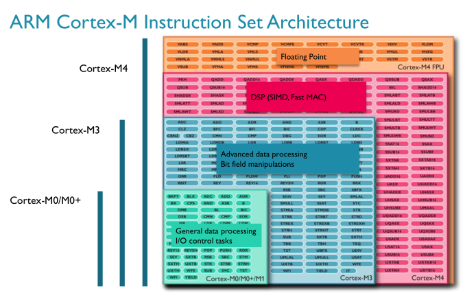
Each Cortex M chip offers a superset of the previous model’s instructions. So a Cortex M3 should theoretically be able to execute code for a Cortex M0+ (but not necessarily vice versa).

You also get support for more interrupts the higher up you go on the Cortex M ladder. The Cortex M0/M0+ designs support up to 32 interrupts, but if you move up to the M3/M4 you get up to 240.

All Cortex M processors have 32-bit memory addressability and the exact same memory map across all designs. ARM’s goal with these chips is to make moving up between designs as painless as possible.

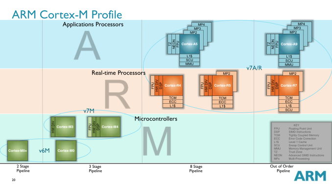
While we’ve spent the past few years moving to out-of-order designs in smartphone CPUs, the entire Cortex M family is made up of very simple, in-order architectures. The pipelines themselves are similarly simplified:

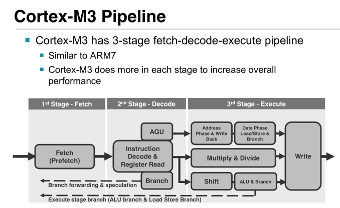
Cortex M0, M3 and M4 all feature 3-stage in-order pipelines, while the M0+ shaves off a stage of the design. In the 3-stage designs there’s an instruction fetch, instruction decode and a single instruction execute stage. In the event the decoder encounters a branch instruction, there’s a speculative instruction fetch that grabs the instruction at the branch target. This way regardless of whether or not the branch is taken, the next instruction is waiting with at most a 1 cycle delay.

These aren’t superscalar designs, there’s only a 1-wide path for instruction flow down the pipeline and not many execution units to exploit. The Cortex M3 and M4 add some more sophisticated units (hardware integer divide in M3, MAC and limited SIMD in M4), but by and large these are simple cores for simple needs.

The range of operating frequencies for these cores is relatively low. ARM typically expects to see Cortex M designs in the 20 – 150MHz range, but the cores are capable of scaling as high as 800MHz (or more) depending on process node. There’s a corresponding increase in power consumption as well, which is why we normally see lower clocked Cortex M designs.

Similar to the Cortex A and R lines, the Cortex M family has a roadmap ahead of it. ARM recently announced a new CPU design center in Taiwan, where Cortex M based cores will be designed. I view the Cortex M line today quite similarly to the early days of the Cortex A family. There’s likely room for a higher performing option in between Cortex M4 and Cortex A7. If/when we get such a thing I feel like we may see the CPU building block necessary for higher performance wearable computing.