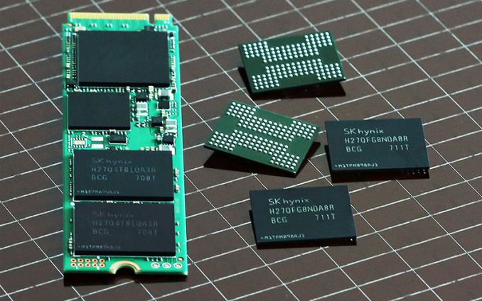
NZXT Releases Kraken G12 Liquid Cooler GPU Mounting Kit
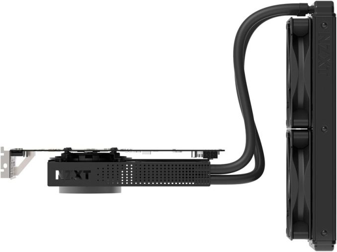
NZXT has announced its Kraken G12 mounting kit, which is designed to allow video cards to mount a closed-loop liquid cooler. In junctionwith a cooler, the adapter can significantly decrease GPU temperatures and improve cooling of VRMs; it is compatible with various coolers and cards.
Closed-loop liquid cooling systems (LCSes) for CPUs have gained popularity among enthusiasts in the recent years due to high efficiency amid relatively small dimensions. But while high-performance GPUs have higher TDPs (and therefore greater heat generation) than advanced CPUs, few LCSes can be attached to graphics cards out of the box. Some companies (e.g., Corsair) offer special adapters (brackets) to make their liquid coolers compatible with popular graphics boards, but NZXT is the one of a few vendors to offer mounting kits that are designed to be compatible not only with the company’s own LCS, but with other popular liquid coolers as well.
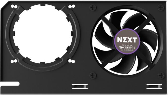
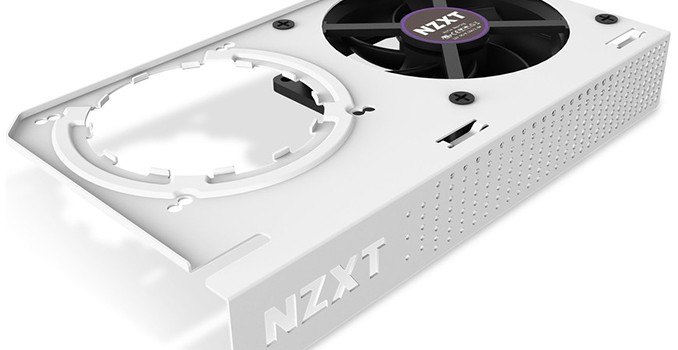
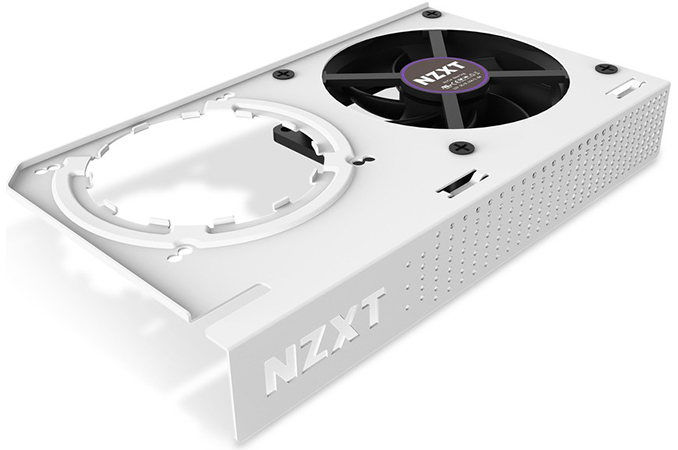
The NZXT Kraken G12 is a relatively simple device that consists of bracket compatible with various waterblocks from NZXT, Corsair, Thermaltake, Antec, and Zalman as well as multiple reference and non-reference graphics cards based on AMD or NVIDIA GPUs (see the table). The Kraken G12 is equipped with a 92-mm fan with up to 1500 RPM speed that can cool down the various video card components that aren’t covered by the LCS, such as DRAM chips and VRM components (inductors, MOSFETs, capacitors, etc.). All of which is important, especially as the latter get very hot under high load.
| NZXT Kraken G12 | |||||
| Matte White RL-KRG12-W1 |
Matte Black RL-KRG12-B1 |
||||
| Dimensions | 201 × 113 × 32 mm | ||||
| Materials | Steel and Plastic | ||||
| Weight | 282 g | ||||
| Fan | 92-mm, 1500 RPM, rifle bearing with 3-pin connector | ||||
| Compatible Graphics Cards | AMD | RX 480, 470, R9 390X*, 390*, 380X*, 380, 290X*, 290*, 285*, 280X*, 280*, 270X, 270, R7 370, HD7970*, 7950*, 7870, 7850, 6970, 6950, 6870, 6850, 6790, 6770, 5870, 5850, 5830
* Some variations in AMD die height may require the use of a copper shim which is not included. |
|||
| NVIDIA | Titan X, Titan, Geforce GTX 1080, 1070, 1060, 980 Ti, 980, 970, 960, 780 Ti, 780, 770, 760, 680, 670, 660Ti, 660, 580, 570 | ||||
| Compatible AIO LCS | Antec | KUHLER H2O 920V4, 620V4, 920, 620 | |||
| Corsair | H105, H110, H90, H75, H55, H50 (CW-906006-WW only) | ||||
| NZXT | Kraken X62, X52, X42, X61, X41, X31, X60, X40 | ||||
| Thermaltake | Water 3.0 Riing RGB 360, 280, 240, Red 280, 140, Water 3.0 Ultimate, Extreme S, Extreme, Pro, Performer Water 2.0 Extreme, Pro, Performer |
||||
| Zalman | LQ-320, LQ-315, LQ-310 | ||||
| Warranty | 2 Years | ||||
In fact, the Kraken G12 is not the first product of the kind from NZXT. Several years ago it released its Kraken G10 bracket for then-contemporary coolers and video cards. The Kraken G12 just expands the list of compatible components, uses a new fan with a lower rotating speed and adds a white option. From a technical point of view, making the Kraken G12 compatible with LCSes from five different suppliers is not a problem as compliant closed-loop liquid coolers are designed for standard CPU sockets and are made by Asetek, so, their constructions are similar.
The NZXT Kraken G12 will be available towards the end of the month for $29 in the USA.


Related Reading:
- NZXT Kraken G10 Review: Liquid Cooling for Your GPU
- Closed Loop AIO Liquid Coolers: 14-way Mega Roundup Review
- Closing the Loop: Contained Liquid-Coolers from Corsair and NZXT Compared
- The NZXT Manta mITX Case Review
- NZXT H440 “EnVyUs” Edition Chassis Announced: H440 Gets an e-Sports Edition
- NZXT Unveils Fully Customizable Aer RGB LED Fans
- Raijintek Shows Off Pumpless Liquid Cooling System