Vik


Qualcomm Announces 205 Mobile Platform: Entry-Level LTE for India & Emerging Markets

Qualcomm Announces 205 Mobile Platform: Entry-Level LTE for India & Emerging Markets

This morning in New Delhi, Qualcomm is taking the wraps off of their latest entry-level, high-volume SoC, the Qualcomm 205 SoC. The cornerstone of the Qualcomm 205 Mobile Platform – and keeping in mind last week’s renaming of Qualcomm’s product stack – the 205 Platform is being launched as Qualcomm’s new entry-level SoC for emerging markets. Qualcomm’s focus on this latest 200-series SoC is bringing an LTE-enabled SoC down to its lowest price point yet, ultimately aiming to get LTE into the sub-$50 mass-market feature phones that are popular in these markets.

Qualcomm’s 200-Series SoC Lineup
  205 SoC 208 SoC 210 SoC
CPU 2 x ARM Cortex A7 @ 1.1GHz 2 x ARM Cortex A7 @ 1.1GHz 4 x ARM Cortex A7 @ 1.1GHz
GPU Adreno 304 Adreno 304 Adreno 304
Memory Interface 32-bit LPDDR2/3 32-bit LPDDR2/3 32-bit LPDDR2/3
Integrated Modem Snapdragon X5: LTE Category 4, HSPA+, DS-DA, VoLTE Gobi 3G: HSPA+, DS-DA Snapdragon X5: LTE Category 4, HSPA+, DS-DA, VoLTE
Integrated WiFi 802.11n 1-stream 802.11n 1-stream 802.11n 1-stream
Manufacturing Process 28nm LP 28nm LP 28nm LP
Video Encode/Decode Decode: 720p30
Encode: 480p30
Decode: 720p
Encode: 720p
Decode: 1080p
Encode: 720p
Launch Date 03/2017 09/2014 09/2014

From a technical perspective, Qualcomm has offered LTE in the 200 series SoCs since the 210 SoC in 2014. However this was on a slightly more premium quad-core CPU design, whereas Qualcomm’s cheapest SoCs are even simpler dual-core designs. The difference comes down a fraction of a dollar, but for emerging markets looking to push out to LTE – and with many of those markets subsidizing phones – even the cents matter. So now Qualcomm is rolling out a dual-core design with LTE, offering an even more basic design than the 3G-only 208 or the LTE-equipped 210.

At a high level, the specs are unremarkable and appropriately simplistic. We’re looking at a dual-core Cortex-A7 CPU running at 1.1GHz and paired up with an Adreno 304 GPU, and, most importantly, one of the company’s X5 LTE modems. The X5 is a basic modem design that offers up to LTE Cat 4 speeds (150Mbps down/50Mbps up), which is more than sufficient for Qualcomm’s goals with LTE for emerging markets. Dual-sim functionality is present, as is VoLTE and VoWiFi as well. Video encode/decode are very basic, offering 720p30 decode and 480p30 encode, with a display controller capable of driving just a VGA (640×480) display, all of which is a notable reduction from the 208/210. The Hexagon DSP has been removed as well, saving further die space. Even the chip itself is designed to save a few pennies on implementation; it’s pin-compatible with the 210/208 so that it can be dropped into existing designs.

Qualcomm’s big push for LTE connectivity in entry-level phones in India and other emerging markets comes as the company expects both consumers and carriers in those markets to make the transition over to LTE, which in turn means phone manufacturers are in need of a cheap platform that can handle LTE. Though the definition of what exactly a feature phone is in 2017 is a bit muddled – the form factor seems to be the only defining element when even the OSes are now full-fledged systems based on ASOP and other Linux projects – they remain the cheapest phones, and Qualcomm expects them to benefit from LTE in similar ways as smartphones have over the last several years.


Underpinning all of this is of course the massive spectrum efficiency gains in LTE versus 3G & 2G communication protocols, which increase the bandwidth available in a given area even without a larger number of towers. Otherwise Qualcomm expects the use cases for feature phones to be many of the same ones as smartphone users already do, if only on a smaller scale: social media, video streaming, etc. Meanwhile, one claim that particularly caught my attention is that Qualcomm is expecting to be able to get 45 day standby out of 205 phones; while 205 is of course designed for low power operation, with a 2000mAh battery this works out to a standby power consumption of just 6mW.

Finally, Qualcomm is noting that the 205 SoC and its associated software were all developed in India, as part of fulfilling the country’s Make in India initiative, which at a couple of years old now, is intended to encourage manufacturers to invest in manufacturing within the country rather than importing finished products. While Make in India and the country’s associated attempts to encourage internal manufacturing have not always been well received – Apple and others have balked at the concept at times – it has been successful in driving semiconductor companies like Qualcomm towards developing entry-level hardware in the country. Though in Qualcomm’s case, the company has operated a development center for a lot longer than just the last couple of years.

Wrapping things up, Qualcomm is shipping the 205 Mobile Platform today. Phones based on the platform will be showing up quickly thereafter, with the first devices expected next quarter.

Qualcomm Announces 205 Mobile Platform: Entry-Level LTE for India & Emerging Markets

Qualcomm Announces 205 Mobile Platform: Entry-Level LTE for India & Emerging Markets

This morning in New Delhi, Qualcomm is taking the wraps off of their latest entry-level, high-volume SoC, the Qualcomm 205 SoC. The cornerstone of the Qualcomm 205 Mobile Platform – and keeping in mind last week’s renaming of Qualcomm’s product stack – the 205 Platform is being launched as Qualcomm’s new entry-level SoC for emerging markets. Qualcomm’s focus on this latest 200-series SoC is bringing an LTE-enabled SoC down to its lowest price point yet, ultimately aiming to get LTE into the sub-$50 mass-market feature phones that are popular in these markets.

Qualcomm’s 200-Series SoC Lineup
  205 SoC 208 SoC 210 SoC
CPU 2 x ARM Cortex A7 @ 1.1GHz 2 x ARM Cortex A7 @ 1.1GHz 4 x ARM Cortex A7 @ 1.1GHz
GPU Adreno 304 Adreno 304 Adreno 304
Memory Interface 32-bit LPDDR2/3 32-bit LPDDR2/3 32-bit LPDDR2/3
Integrated Modem Snapdragon X5: LTE Category 4, HSPA+, DS-DA, VoLTE Gobi 3G: HSPA+, DS-DA Snapdragon X5: LTE Category 4, HSPA+, DS-DA, VoLTE
Integrated WiFi 802.11n 1-stream 802.11n 1-stream 802.11n 1-stream
Manufacturing Process 28nm LP 28nm LP 28nm LP
Video Encode/Decode Decode: 720p30
Encode: 480p30
Decode: 720p
Encode: 720p
Decode: 1080p
Encode: 720p
Launch Date 03/2017 09/2014 09/2014

From a technical perspective, Qualcomm has offered LTE in the 200 series SoCs since the 210 SoC in 2014. However this was on a slightly more premium quad-core CPU design, whereas Qualcomm’s cheapest SoCs are even simpler dual-core designs. The difference comes down a fraction of a dollar, but for emerging markets looking to push out to LTE – and with many of those markets subsidizing phones – even the cents matter. So now Qualcomm is rolling out a dual-core design with LTE, offering an even more basic design than the 3G-only 208 or the LTE-equipped 210.

At a high level, the specs are unremarkable and appropriately simplistic. We’re looking at a dual-core Cortex-A7 CPU running at 1.1GHz and paired up with an Adreno 304 GPU, and, most importantly, one of the company’s X5 LTE modems. The X5 is a basic modem design that offers up to LTE Cat 4 speeds (150Mbps down/50Mbps up), which is more than sufficient for Qualcomm’s goals with LTE for emerging markets. Dual-sim functionality is present, as is VoLTE and VoWiFi as well. Video encode/decode are very basic, offering 720p30 decode and 480p30 encode, with a display controller capable of driving just a VGA (640×480) display, all of which is a notable reduction from the 208/210. The Hexagon DSP has been removed as well, saving further die space. Even the chip itself is designed to save a few pennies on implementation; it’s pin-compatible with the 210/208 so that it can be dropped into existing designs.

Qualcomm’s big push for LTE connectivity in entry-level phones in India and other emerging markets comes as the company expects both consumers and carriers in those markets to make the transition over to LTE, which in turn means phone manufacturers are in need of a cheap platform that can handle LTE. Though the definition of what exactly a feature phone is in 2017 is a bit muddled – the form factor seems to be the only defining element when even the OSes are now full-fledged systems based on ASOP and other Linux projects – they remain the cheapest phones, and Qualcomm expects them to benefit from LTE in similar ways as smartphones have over the last several years.


Underpinning all of this is of course the massive spectrum efficiency gains in LTE versus 3G & 2G communication protocols, which increase the bandwidth available in a given area even without a larger number of towers. Otherwise Qualcomm expects the use cases for feature phones to be many of the same ones as smartphone users already do, if only on a smaller scale: social media, video streaming, etc. Meanwhile, one claim that particularly caught my attention is that Qualcomm is expecting to be able to get 45 day standby out of 205 phones; while 205 is of course designed for low power operation, with a 2000mAh battery this works out to a standby power consumption of just 6mW.

Finally, Qualcomm is noting that the 205 SoC and its associated software were all developed in India, as part of fulfilling the country’s Make in India initiative, which at a couple of years old now, is intended to encourage manufacturers to invest in manufacturing within the country rather than importing finished products. While Make in India and the country’s associated attempts to encourage internal manufacturing have not always been well received – Apple and others have balked at the concept at times – it has been successful in driving semiconductor companies like Qualcomm towards developing entry-level hardware in the country. Though in Qualcomm’s case, the company has operated a development center for a lot longer than just the last couple of years.

Wrapping things up, Qualcomm is shipping the 205 Mobile Platform today. Phones based on the platform will be showing up quickly thereafter, with the first devices expected next quarter.

Intel Introduces Optane SSD DC P4800X With 3D XPoint Memory

Intel Introduces Optane SSD DC P4800X With 3D XPoint Memory

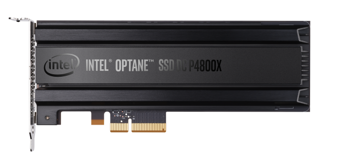
A year and a half after first publicly unveiling their new 3D XPoint non-volatile memory technology, Intel is launching the first product incorporating the new memory. The Intel Optane SSD DC P4800X is an enterprise PCIe 3 x4 NVMe SSD that Intel promises will be the the most responsive data center SSD with lower latency than all of the fastest NAND flash based competitors. After months of touting 3D XPoint memory primarily with rough order of magnitude claims about its performance, endurance and cost relative to DRAM and NAND flash, and after some unexplained delays, Intel is finally providing some concrete specifications and pricing for a complete SSD that is shipping today. The information is more limited than we’re accustomed to for their NAND flash SSDs, and Intel still isn’t confirming anything about the materials or exact operating principle of the 3D XPoint memory cell.

Current computer system architectures are based around the use of DRAM as working memory and NAND flash for fast storage. 3D XPoint memory falls between the two technologies on most important metrics, so Optane SSDs bring a new dimension of complication to a server architect’s task. For most enterprise use cases, the most enticing feature of Optane SSDs over NAND SSDs is the former’s higher performance, especially reduced latencies. Aside from the gains from switching to the NVMe protocol, the latency offered by NAND flash based SSDs has been mostly stagnant or even regressed with the disappearance of SLC NAND from the market, even as throughput and capacity have grown with every generation.

The Intel Optane SSD DC P4800X is rated for a typical read or write latency under 10µs, compared to tens of microseconds for the best NAND flash based SSDs, and about 4µs minimum imposed by PCIe and NVMe transaction overhead. More impressive is how little latency degrades under less than ideal conditions. Queue depth 1 random reads are rated to remain below 30µs even while the drive is simultaneously accepting 2GB/s of sustained random writes (about 500k IOPS). Intel even specifies Quality of Service (QoS) standards for latency at the 99.999th percentile, with even QD16 random writes staying almost entirely below 200µs. A consequence of the low latency is that the P4800X can deliver full throughput at lower queue depths: the P4800X is rated to deliver maximum IOPS at QD16 while flash-based SSDs are specified for queue depths of at least 32. Unlike flash memory, the read and write performance of 3D XPoint memory is roughly equal, and this is reflected in Intel’s specifications for the P4800X.

Conspicuously missing from the performance specifications are sequential throughput. The P4800X can already use more than half of the available PCIe bandwidth with a completely random I/O workload. Rather than reassure us that the P4800X can do even better with larger transfer sizes, Intel suggests that being overly concerned with the sequential transfer speeds is a sign that you should be shopping for their 3D NAND SSDs instead. They’ll offer plenty of throughput for a far lower price.

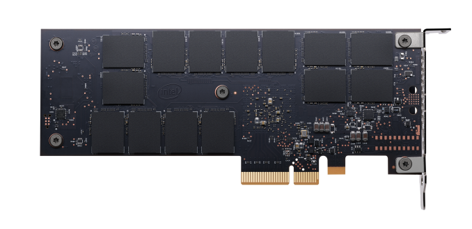
Intel’s 3D XPoint memory is being manufactured as a 128Gb (16GB) die, slightly behind the trend for NAND flash capacities. As a result, the Optane SSD DC P4800X will start with a 375GB model and later this year be followed by 750GB and 1.5TB models. The top-performing enterprise SSDs currently tend to be multi-TB drives. Intel has shared very few details about the new controller they’ve developed for the P4800X, but they have disclosed that the 375GB model uses seven channels with four dies per channel, for a total of 28 chips and a raw capacity of 448GB. Fourteen packages of 3D XPoint memory are visible on the back side of the drive in the photographs Intel has released, suggesting that fourteen more packages are hiding under the heatsink and that the 375GB add-in card model is using single-die packages. The controller implements a high-performance all-hardware read path that does not involve the drive’s firmware, and while the exact stride of memory accesses is not known, a single 4k read will be spread across all seven channels.

3D XPoint memory can be read or written with byte granularity and modifications can be written in place, so it is free from the worst internal fragmentation and write amplification challenges that are caused by the large page sizes and huge erase block sizes of NAND flash. This means that further overprovisioning beyond the drive’s native amount will have minimal impact on performance and that the performance of a full drive should not suffer severely the way flash based SSDs do. However, some amount of spare area is still required for error correction and other metadata and for a pool of spare blocks to replace failed or defective blocks. The write endurance of 3D XPoint memory is not infinite so wear leveling is still required, but it is a much simpler process that requires much less spare area.

The Intel Optane SSD DC P4800X has a write endurance rating of 30 Drive Writes Per Day, and Intel is hopeful that future products can offer even higher ratings once 3D XPoint memory has more broadly proven its reliability. Today’s limited release 375GB models have a three year warranty for a total write endurance rating of 12.3 PB, and once the product line is expanded to broad availability of the full range of capacities in the second half of this year the warranty period will be five years.

Intel is offering the 375GB P4800X in PCIe add-in card form factor with a MSRP of $1520 starting today with a limited early-ship program. In Q2 a 375GB U.2 model will ship, as well as a 750GB add-in card. In the second half of the year the rest of the capacity and form factor options will be available, but prices and exact release dates for those models have not been announced. At just over $4/GB the P4800X seems to fall much closer to DRAM than NAND in price, though to be fair the enterprise SSDs it will compete against are all well over $1/GB and the largest DDR4 DIMMs are around $10/GB.

Intel Optane SSD DC P4800X Specifications
Capacity 375 GB 750 GB 1.5 TB
Form Factor PCIe HHHL or 2.5″ 15mm U.2
Interface PCIe 3.0 x4 NVMe
Controller Intel unnamed
Memory 128Gb 20nm Intel 3D XPoint
Typical Latency (R/W) <10µs
Random Read (4 KB) IOPS (QD16) 550k TBA TBA
Random Read 99.999% Latency (QD1) 60µs TBA TBA
Random Read 99.999% Latency (QD16) 150µs TBA TBA
Random Write (4 KB) IOPS (QD16) 500k TBA TBA
Random Write 99.999% Latency (QD1) 100µs TBA TBA
Random Write 99.999% Latency (QD16) 200µs TBA TBA
Endurance 30 DWPD
Warranty 5 years (3 years during early limited release)
MSRP $1520 TBA TBA
Release Date March 19 (HHHL)
Q2 2017 (U.2)
Q2 2017 (HHHL)
2H 2017 (U.2)
2H 2017


Intel Memory Drive Technology

Along with the DC P4800X, Intel is launching Intel Memory Drive Technology software as a paid add-on. The Memory Drive Technology software is a custom virtual memory system implemented as a minimal hypervisor. The guest operating system or general-purpose hypervisor is presented with the illusion that a portion of the 3D XPoint memory on the Optane SSD is directly addressable, producing an apparent memory capacity that far exceeds the capacity of the system’s installed DRAM. Under the hood and almost entirely transparent to the guest OS, Intel Memory Drive Technology monitors memory access patterns to cache actively used data in DRAM and prefetch from Optane SSDs. At a high level, this is merely duplicating the paging mechanisms all operating systems already provide. However, Intel claims that the heuristics used by Memory Drive Technology can far outperform those currently used by operating systems to manage swap space residing on storage that is far slower than Optane SSDs. On some workloads Intel Memory Drive Technology can offer performance approaching that of an all-DRAM memory pool of equal capacity, though this will depend highly on the specific application workload.

Intel Memory Drive Technology has a substantial capacity overhead: a 375GB Optane SSD can provide up to 320GB of virtual memory. Multiple Optane SSDs can be used to provide virtual memory up to ten times the system’s DRAM capacity, though Intel recommends Optane to DRAM ratios between 3:1 and 8:1. When multiple CPUs or Optane SSDs are in use, the Memory Drive Technology software will take into account non-uniform memory access (NUMA) effects and attempt to optimize data placement to put data in the DRAM or Optane SSD that is closest to the core using it. By default, the Memory Drive Technology software will present to the guest OS a NUMA topology equivalent to the underlying DRAM configuration plus a pool of memory that is not local to any of the processors, with capacity equal to the virtual memory provided by the Optane SSDs. However, this is implemented purely for the sake of allowing NUMA-aware software to adapt its usage patterns; regardless of the NUMA configuration seen by the guest software, the Memory Drive Technology software will not be statically allocating specific address ranges to DRAM or Optane storage. The approach taken by the Memory Drive Technology software allows operating systems and applications to function without modification and without requiring Optane-specific optimizations, but it also means there is no way for applications that are NUMA-aware or use system calls like madvise to communicate directly with the real memory allocator.

The full licensing cost structure for Intel Memory Drive Technology is not clear, but the MSRP for a 375GB P4800X bundled with Memory Drive Technology is $1951 compared to $1520 for the SSD alone. The Memory Drive Technology hypervisor must be booted from a USB device or an IDE-compatible storage controller, and the guest operating system cannot be booted in UEFI mode. Intel Xeon E5-x6xx v2 or later and E7- x8xx v2 or later processors are supported.

Future 3D XPoint-based Optane products on Intel’s roadmap include Optane Memory cache drives for the client/consumer segment, due in Q2 of this year. They will also be followed by larger Optane SSDs for the client market. DIMMs featuring 3D XPoint memory are planned for 2018.