Everspin Announces New MRAM Products And Partnerships
Magnetoresistive RAM manufacturer Everspin has announced their first MRAM-based storage products and issued two other press releases about recent accomplishments. Until now, Everspin’s business model has been to sell discrete MRAM components, but they’re introducing a NVMe SSD based on their MRAM. Everspin’s MRAM is one of the highest-performing and most durable non-volatile memory technologies on the market today, but its density and capacity falls far short of NAND flash, 3D XPoint, and even DRAM. As a result, use of MRAM has largely been confined to embedded systems and industrial computing that need consistent performance and high reliability, but have very modest capacity requirements. MRAM has also seen some use as a non-volatile cache or configuration memory in some storage array controllers. The new nvNITRO family of MRAM drives is intended to be used as a storage accelerator: a high-IOPS low-latency write cache or transaction log, with performance exceeding that of any single-controller drive based on NAND flash.
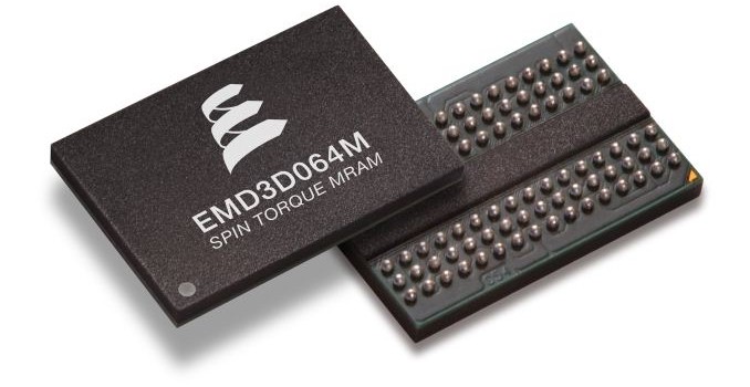
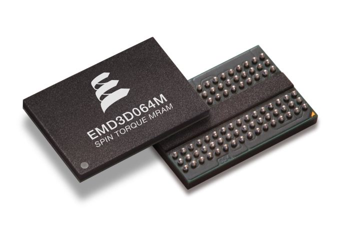
Everspin’s current generation of spin-torque MRAM has a capacity of 256Mb per die with a DDR3 interface (albeit with very different timings from JEDEC standard for DRAM). The initial nvNITRO products will use 32 or 64 MRAM chips to offer capacities of 1GB or 2GB on a PCIe 3 x8 card. MRAM has high enough endurance that the nvNITRO does not need to perform any wear leveling, which allows for a drastically simpler controller design and means performance does not degrade over time or as the drive is filled up—the nvNITRO does not need any large spare area or overprovisioning. Read and write performance are also nearly identical, while flash memory suffers from much slower writes than reads, which forces flash-based SSDs to buffer and combine writes in order to offer good performance. Everspin did not have complete performance specifications available at time of writing, but the numbers they did offer are very impressive: 6µs overall latency for 4kB transfers (compared to 20µs for the Intel SSD DC P3700), and 1.5M IOPS (4kB) at QD32 (compared to 1.2M IOPS read/200k IOPS write for the HGST Ultrastar SN260). The nvNITRO does rely somewhat on higher queue depths to deliver full performance, but it is still able to deliver over 1M IOPS at QD16, around 800k IOPS at QD8, and QD1 performance is around 175k IOPS read/150k IOPS write. MRAM supports fine-grained access, so the nvNITRO performs well even with small transfer sizes: Everspin has hit 2.2M IOPS for 512B transfers, although that is not an official performance specification or measurement from the final product.
As part of today’s announcements, Everspin is introducing MRAM support for Xilinx UltraScale FPGAs in the form of scripts for Xilinx’s Memory Interface Generator tool. This will allow customers to integrate MRAM into their designs as easily as they would use SDRAM or SRAM. The nvNITRO drives are a demonstration of this capability, as the SSD controller is implemented on a Xilinx FPGA. The FPGA provides the PCIe upstream link as a standard feature, the memory controller is Everspin’s new and Everspin has developed a custom NVMe implementation to take advantage of the low latency and simple management afforded by MRAM. Everspin claims a 30% performance advantage over an unspecified NVRAM drive based on battery-backed DRAM, and attributes it primarily to their lightweight NVMe protocol implementation. In addition to NVMe, the nvNITRO can be configured to allow all or part of the memory to be directly accessible for memory-mapped IO, bypassing the protocol overhead of NVMe.
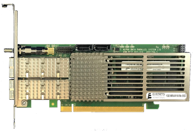
The initial version of the nvNITRO is built with an off-the-shelf FPGA development board and mounts the MRAM on a pair of SO-DIMMs. Later this year Everspin will introduce new denser versions on a custom PCIe card, as well as M.2 drives and 2.5″ U.2 using a 15mm height to accommodate two stacked PCBs. By the end of the year, Everspin will be shipping their next generation 1Gb ST-MRAM with a DDR4 interface, and the nvNITRO will use that to expand to capacities of up to 16GB in the PCIe half-height half-length card form factor, 8GB in 2.5″ U.2, and at least 512MB for M.2.
Everspin has not announced pricing for the nvNITRO products. The first generation nvNITRO products are currently sampling to select customers and will be for sale in the second quarter of this year, primarily through storage vendors and system integrators as a pre-installed option.
New Design Win For Current MRAM
Everspin is also announcing another design win for their older field-switched MRAM technology. JAG Jakob Ltd is adopting Everspin’s 16Mb MRAM parts for their PdiCS process control systems, with MRAM serving as both working memory and code storage. These systems have extremely strict uptime requirements, hard realtime performance requirements and service lifetimes of up to 20 years; there are very few memory technologies on the market that can satisfy all of those requirements. Everspin will continue to develop their line of MRAM devices that compete against SRAM and NOR flash even as their higher-capacity offerings adopt DRAM-like interfaces.