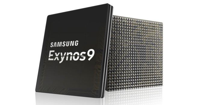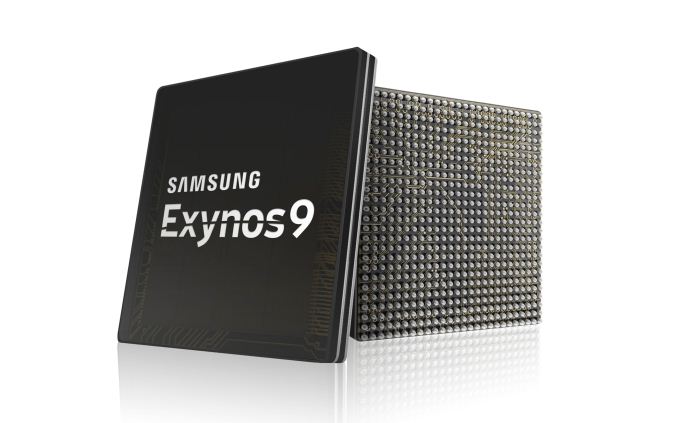
Even though Mobile World Congress doesn’t kick off for another few days, Samsung isn’t wasting any time in getting started. This morning the company is announcing their latest generation high-end ARM SoC, the Exynos 8895. Their first in-house 10nm SoC, the company isn’t talking about what it will go in, but based on the context of the announcement it’s a safe bet we’re looking at the SoC for at least some SKUs of the next Galaxy S phone.
While Samsung has been in the SoC game with the Exynos series for a number of years now, it’s been in the last few years that they’ve really cemented their positon as a market leader at the high-end. Thanks in part to the company’s 14nm process, the Exynos 7420 proved to be a very capable and powerful SoC from the company. Last year Samsung followed that up with the Exynos 8890, which among other firsts marked Samsung’s entry into designing their own CPU cores with the M1.
Now for 2017 Samsung wants to repeat their success over the past couple of years with the Exynos 9 Series 8895. As you can likely infer from the name, it’s not meant to be radically different from the preceding 8890, but there are still some pretty important changes here that should affect performance across the board.
| Samsung Exynos SoCs Specifications |
| SoC |
Exynos 8895 |
Exynos 8890 |
Exynos 7420 |
| CPU |
4x A53
4x Exynos M2(?) |
4x [email protected]
4x Exynos M1 @ 2.3GHz |
4x [email protected]
4x [email protected] |
| GPU |
Mali G71MP20 |
Mali T880MP12
@ 650MHz |
Mali T760MP8
@ 770MHz |
Memory
Controller |
2x 32-bit(?)
LPDDR4x
|
2x 32-bit
LPDDR4 @ 1794MHz
28.7GB/s b/w |
2x 32-bit
LPDDR4 @ 1555MHz
24.8GB/s b/w |
| Storage |
eMMC 5.1, UFS 2.1 |
eMMC 5.1, UFS 2.0 |
eMMC 5.1, UFS 2.0 |
| Modem |
Down: LTE Cat16
Up: LTE Cat13 |
Down: LTE Cat12
Up: LTE Cat13 |
N/A |
| ISP |
Rear: 28MP
Front: 28MP |
Rear: 24MP
Front: 13MP |
Rear: 16MP
Front: 5MP |
Mfc.
Process |
Samsung
10nm LPE |
Samsung
14nm LPP |
Samsung
14nm LPE |
The big deal for Samsung of course is that the Exynos 8895 is their first 10nm SoC, designed by Samsung LSI and fabbed by Samsung. Semantics of what is or isn’t 10nm aside, Samsung’s 10nm LPE process is cutting-edge for a mobile SoC, and relative to the current 14nm process offers better density and better performance characteristics. Samsung has talked about the process a bit in the past, and for the Exynos 8895 announcement they are reiterating that the 10nm LPE process offers “up to 27% higher performance while consuming 40% less power” relative to 14nm. However this may be in error in phrasing on Samsung’s part, as last year it was “27-percent higher performance or 40-percent lower power consumption”, which is a more realistic statement. Either way, for 8895 in particular, Samsung isn’t talking about performance quite yet.
Diving into the specs, the CPU situation looks a great deal like the previous 8890. Samsung has gone with 8 cores – 4 high-power, 4 low-power – with a mix of custom and licensed silicon. The high-power cores are composed of what Samsung is calling a “2nd generation” custom CPU core. This would presumably be a newer iteration of the M1 (so the M2?), but Samsung isn’t offering up much in the way of details at this time over what’s changed from the M1. What we do know is that Samsung is touting that it offers both better performance and improved energy efficiency. Meanwhile low-power work is once again being provided by ARM’s Cortex-A53. (ed: which on 10nm, must be absolutely tiny, considering that a core was sub-1mm2 on 14nm)
Meanwhile on the GPU side, Samsung has significantly upgraded their graphics capabilities by tapping ARM’s latest-generation Mali-G71 GPU in an MP20 configuration. Based on ARM’s new Bifrost GPU architecture, the G71 radically overhauls the internal workings of the GPU to match the contemporary thread level parallelism (TLP)-centric nature of desktop GPUs and modern workloads. ARM has previously discussed that they expect G71-based devices to offer around 50% better graphics performance than T880 devices, and Samsung is going one step further by touting it as 60% faster performance.

In another first for Samsung, the 8895 is also their first Heterogeneous System Architecture (HSA) compliant SoC. This requires that the CPU, GPU, and interconnect all support HSA, and indeed all of the necessary pieces have come together for 8895. We’ve previously seen that the Mali-G71 GPU is HSA-compliant, and meanwhile for the 8895 Samsung has rolled out a new version of their interconnect (the Samsung Coherent Interconnect) to support HSA. This isn’t a development that I expect will have immediate ramifications, but HSA is ultimately at the core of making it easier for developers to program applications that use the GPU in a compute context, thanks to the common (and common-sense) architecture rules for HSA.
To feed the resulting beast, Samsung has added support for LPDDR4x memory. An extension of the original LPDDR4 standard, LPDDR4x is designed to reduce DRAM power consumption by up to 20% by reducing the output driver power (I/O VDDQ voltage) by 45%, from 1.1 V to 0.6 V. LPDDR4x memory has just started shipping, so along with the previously announced Snapdragon 835, the Exynos 8895 is the other high-performance SoC coming out this year to support the new memory.

The Exynos 8895 is also getting an upgraded ISP. The latest ISP supports 28MP for both the front and rear cameras, while a bit more nebulously, Samsung’s spec sheet also lists support for “28MP+16MP Dual Camera” mode, an unsurprising development given the recent popularity of dual camera phone designs. Diving a bit deeper, we find that the 8895’s ISP is actually two ISPs: a high-performance ISP and a low-power ISP, with the low-power ISP presumably providing the aforementioned 16MP capability. Samsung is touting this combination as allowing them to offer dual camera functionality while still keeping power consumption in check.
On the flip slide of the coin, the Exynos 8895 also gets a new version of Samsung’s video decode block, which the company calls their Multi-Format Codec (MFC). This latest MFC supports all the bells and whistles you’d expect, with both HEVC and VP9 decoding up to 4Kp120. Samsung’s press release also briefly mentions a “video processing technology that enables a higher quality experience by enhancing the image quality” that’s capable of “enhancing the image quality of a specific portion that is perceived more sensitive to the human eye.” Given the VR applications – and Samsung wants to be able to do 4K VR – this sounds a bit like a variation on the idea of foveated rendering, but there aren’t any further details on the technology at this time.
Also appearing for the first time on the Exynos 8895 is Samsung’s Cat16 LTE modem design. With their modem Samsung is using 5x Carrier Aggregation to achieve up to 1Gbps down, while uploading is rated at LTE Cat 13, using 2 carriers to get 150Mbps up. What’s notable here is that, as best as I can tell, this is the first modem using 5x CA; Qualcomm’s equivalent modem, the X16, uses 3 or 4x CA depending on the scenario. Unfortunately with the limited details Samsung offers right now, I’m not sure whether they have to use 5x CA to get Cat 16 bandwidth, or this is just another optional mode.

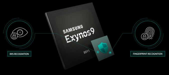
Finally, the Exynos 8895 also includes what Samsung is calling an “enhanced security sub-system with a separate security processing unit” for use with user authentication, mobile payments, and the like. Based on Samsung’s description this sounds a heck of a lot like Apple’s Secure Enclave, which would be a very welcome development, as in Apple’s case it has made their phones a lot harder to break into.
Wrapping things up, along with today’s product announcement of the Exynos 8895, Samsung is also announcing that the SoC is in mass production; and indeed I would be surprised if this isn’t the SoC they announced back in October, which would mean it’s been in production for some time now. We still don’t know when we’re going to see the next Samsung Galaxy S phone, but given how Samsung is announcing the SoC in this fashion, clearly it’s going to be sooner than later. In the meantime, hopefully we’ll get some additional SoC details next week at MWC.