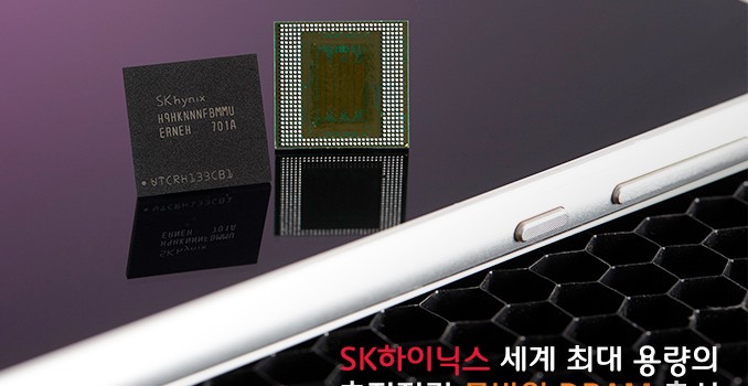
SK Hynix Announces 8 GB LPDDR4X-4266 DRAM Packages
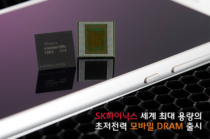
SK Hynix on Monday officially announced the industry’s first 8 GB LPDDR4X (LP4X) packages for next-generation mobile devices. The new memory chips not only increase DRAM performance but also reduce its power consumption due to lower I/O voltages (and come in a smaller form-factor). Interested parties have already obtained samples of SK Hynix’s LPDDR4X ICs and the first devices featuring the new type of memory are expected to hit the market in the coming months.
The LPDDR4X is a new mobile DRAM standard that is an extension of the original LPDDR4, and is expected to reduce power consumption of the DRAM sub-system by 18~20% according to developers (everything else remains the same: a 200~266 MHz internal memory array frequency, 16n prefetch, etc.). To do that, LPDDR4X cuts output driver power (I/O VDDQ voltage) by 45%, from 1.1 V to 0.6 V. LPDDR4X is supported by a number of mobile SoC developers. The first application processor to support the new type of memory is MediaTek’s Helio P20 that was announced nearly a year ago and the initial devices powered by the chip are likely to hit the market in 1H 2017. Another notable SoC to support LPDDR4X is Qualcomm’s new flagship Snapdragon 835, which was announced in November and detailed earlier this month. Smartphones featuring this chip will not show up for a while, but MWC just around the corner which lends nicely to various handset announcements.

The 8 GB (64 Gb) LPDDR4X package stacks four 16 Gb DRAM parts that feature a 4266 MT/s data transfer rate and provide up to 34.1 GB/s of bandwidth when connected to an application processor using a 64-bit memory bus. For its 8 GB LPDDR4X solution SK Hynix uses a new 12 mm × 12.7 mm BGA package, which is 30% smaller compared to standard LPDDR4 stacks that come in 15 mm × 15 mm form-factor. SK Hynix’s 8 GB LPDDR4X solution has a thickness of less than 1 mm to enable PoP stacking with a mobile application processor or a UFS NAND storage device.
| SK Hynix 8 GB LPDDR4X DRAM Packages | ||||||
| H9HKNNNFBUMU ERNEH |
H9HKNNNFBMMUDR | H9HKNNNEBMMUER | H9HKNNNEBMAUDR | |||
| DRAM IC Capacity | 16 Gb | 12 Gb | ||||
| Number of DRAM ICs | 4 | |||||
| Package Capacity | 64 Gb (8 GB) | 48 Gb (6 GB) | ||||
| Data Rate | 4266 MT/s | 3733 MT/s | ||||
| Bus Width | x64 | |||||
| Bandwidth | 34.1 GB/s | 29.8 GB/s | 29.8 GB/s | |||
| Package | FBGA | FBGA-376 | FBGA-366 | FBGA-376 | ||
| Dimensions | 12 mm × 12.7 mm | |||||
| Voltages | 1.8V / 1.1V / 0.6V | |||||
| Process Technology | 21 nm | |||||
| Availability | 2017 | |||||
SK Hynix did not announce exact power consumption figures for its LP4X parts, but confirmed that the reduction of I/O voltage by 45% reduces power consumption of the whole memory sub-system by around 20% versus a hypothetical LPDDR4 memory sub-system running at the frequency in the same conditions. This is not exactly a good description because SK Hynix’s LPDDR4 offerings top at 3733 MT/s. Assuming that the manufacturer did not optimize the design of its LPDDR4X DRAM arrays to reduce power consumption, but only reduced VDDQ to 0.6 V, a memory sub-system based on the new 8 GB LP4X-4266 part should consume less than a similar sub-system running the company’s 8 GB LP4-3733 stack, but the exact figure is unknown.

To make its 16 Gb LPDDR4X memory ICs, SK Hynix uses its 21 nm fabrication process, which is also used to manufacture 16 Gb LPDDR4 ICs. So, from manufacturing technology standpoint, SK Hynix’s LP4X chips are similar to its LP4 chips.
Initially, SK Hynix will offer only 8 GB LPDDR4X packages with 4266 MT/s data transfer rate based on its 16 Gb DRAM ICs. Eventually, the company intends to expand the lineup with 6 GB/8 GB LPDDR4X-3733 (these are already listed in the company’s Q1 databook) and LPDDR4X-3200 solutions as well as parts based on 8 Gb LPDDR4X ICs (these are not listed in the official documents, but are mentioned in the company’s official blog post). The latter make a lot of sense as far not all mobile are going to use 8 GB of DRAM this year. SK Hynix quotes researchers from IHS Markit, who believe that an average high-end smartphone this year is going to integrate 3.5 GB of memory on average (a mix of 3GB, 4GB, 6GB and 8GB solutions on Android). Meanwhile, keep in mind that DRAM requirements for Apple’s iOS and Google’s Android are different, which is why smartphones running the latter need more memory and handsets featuring 4 GB of Mobile DRAM are going to become mainstream in 2017. By contrast, Apple’s iPhone 7 and iPhone 7 Plus have 2 GB and 3 GB of DRAM, respectively.
SK Hynix said that its 8 GB LPDDR4X-4266 packages are already in mass production. Mobile devices based on the new memory are expected to arrive in the coming months and it is highly likely that select manufacturers may demonstrate their MediaTek Helio P20- and LPDDR4X-based products at MWC next month.
Related Reading: