Vik


Samsung SSD Update: 48-layer 256Gbit TLC 3D NAND & Three New TLC SSDs Announced

Samsung SSD Update: 48-layer 256Gbit TLC 3D NAND & Three New TLC SSDs Announced

When Samsung took the stage at the 2015 Flash Memory Summit, they admittedly didn’t deliver any bombshell announcements on the scale of the Intel/Micron 3D XPoint surprise, but they still had a lot to talk about.

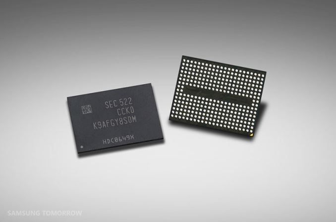
We knew that Samsung’s third generation of V-NAND/3D NAND was on the way with mass production scheduled for the second half of this year. Samsung has now disclosed that mass production is starting this month, and that it’s a 48-layer design with a 256Gb TLC being the first die announced. Samsung’s current second-generation 3D NAND is a 32-layer design available as 128Gb TLC or 128Gb MLC.

With mass production imminent, Samsung has ensured that neither SK Hynix nor the Toshiba/SanDisk joint venture will be able to leapfrog them with their respective 48-layer 3D NAND designs, both scheduled for mass production starting in 2016.

Samsung says the new 256Gb TLC will have about 30% lower power consumption than an equivalent capacity of their current 128Gb TLC, and a switch to a dual-plane organization ensures that one 256Gb die will perform at least as well as a pair of the current 128Gb dies. Density is improved by about 40% while production costs only increased slightly, so price per GB will be going down. At FMS, Samsung is pushing the idea that their 3D NAND TLC is ready to replace MLC for most uses, and they’re optimistic about scaling up their 3D NAND layer count past 100.

New Samsung 48-Layer TLC SSDs
Drive PM953 PM1633 PM1725
Form Factor NVMe over M.2 22110 and 2.5″ 2.5″ SAS 12Gb/s NVMe PCIe HHHL card
Capacities 480GB, 960GB, 1.92TB (2.5″ only) 480GB, 960GB, 1.92TB, 3.84TB 3.2TB, 6.4TB
Sequential Read ? 1,100 MB/s 5,500 MB/s
Sequential Write ? 1,000 MB/s 1,800 MB/s
4kB Random Read IOPS ? 160k 1,000k
4kB Random Write IOPS ? 18k 120k
Endurance Rating ? ? 5 DWPD (6.4 TB model)

Samsung also shared information about three upcoming drives, all using TLC though not necessarily the new 48-layer parts. The PM1633 Enterprise SAS drive was previewed at CES in January and is intended for read-heavy workloads. A follow-on PM1633a model was mentioned to use the new 48-layer TLC to reach 15.36TB capacity, but we don’t have any other information about that update. The PM953 is a enterprise NVMe drive in M.2 or 2.5″ form factors, and is the counterpart to the MLC-based SM951. Of particular interest, the M.2 version is using the M.2 22110 form factor (22mm x 110mm, the maximum length for M.2), with Samsung using the extra space to implement power loss protection.

Meanwhile the PM1725 is a fast multi-TB PCIe expansion card that Samsung intends to use to challenge the assumptions about what uses TLC is suited for. Relatively speaking it appears to be intended for workloads that aren’t very write-heavy, but it still manages 120k IOPS for writes. That just looks small compared to 1M IOPS for reads and a sequential read speed of 5.5GB/s.

All three drives are intended for OEMs, but the PM953 will probably find its way into the retail channel just like the SM951.

Finally, along with Samsung’s new 3D NAND appearing in the afformentioned new drives, it will also be appearing in at least one of their existing drives. The 850 EVO, Samsung’s current consumer TLC drive, will apparently be getting an update to use the new 48-layer TLC, though it’s not clear if this will be new capacities and/or a wholesale NAND update.

Samsung SSD Update: 48-layer 256Gbit TLC 3D NAND & Three New TLC SSDs Announced

Samsung SSD Update: 48-layer 256Gbit TLC 3D NAND & Three New TLC SSDs Announced

When Samsung took the stage at the 2015 Flash Memory Summit, they admittedly didn’t deliver any bombshell announcements on the scale of the Intel/Micron 3D XPoint surprise, but they still had a lot to talk about.

We knew that Samsung’s third generation of V-NAND/3D NAND was on the way with mass production scheduled for the second half of this year. Samsung has now disclosed that mass production is starting this month, and that it’s a 48-layer design with a 256Gb TLC being the first die announced. Samsung’s current second-generation 3D NAND is a 32-layer design available as 128Gb TLC or 128Gb MLC.

With mass production imminent, Samsung has ensured that neither SK Hynix nor the Toshiba/SanDisk joint venture will be able to leapfrog them with their respective 48-layer 3D NAND designs, both scheduled for mass production starting in 2016.

Samsung says the new 256Gb TLC will have about 30% lower power consumption than an equivalent capacity of their current 128Gb TLC, and a switch to a dual-plane organization ensures that one 256Gb die will perform at least as well as a pair of the current 128Gb dies. Density is improved by about 40% while production costs only increased slightly, so price per GB will be going down. At FMS, Samsung is pushing the idea that their 3D NAND TLC is ready to replace MLC for most uses, and they’re optimistic about scaling up their 3D NAND layer count past 100.

New Samsung 48-Layer TLC SSDs
Drive PM953 PM1633 PM1725
Form Factor NVMe over M.2 22110 and 2.5″ 2.5″ SAS 12Gb/s NVMe PCIe HHHL card
Capacities 480GB, 960GB, 1.92TB (2.5″ only) 480GB, 960GB, 1.92TB, 3.84TB 3.2TB, 6.4TB
Sequential Read ? 1,100 MB/s 5,500 MB/s
Sequential Write ? 1,000 MB/s 1,800 MB/s
4kB Random Read IOPS ? 160k 1,000k
4kB Random Write IOPS ? 18k 120k
Endurance Rating ? ? 5 DWPD (6.4 TB model)

Samsung also shared information about three upcoming drives, all using TLC though not necessarily the new 48-layer parts. The PM1633 Enterprise SAS drive was previewed at CES in January and is intended for read-heavy workloads. A follow-on PM1633a model was mentioned to use the new 48-layer TLC to reach 15.36TB capacity, but we don’t have any other information about that update. The PM953 is a enterprise NVMe drive in M.2 or 2.5″ form factors, and is the counterpart to the MLC-based SM951. Of particular interest, the M.2 version is using the M.2 22110 form factor (22mm x 110mm, the maximum length for M.2), with Samsung using the extra space to implement power loss protection.

Meanwhile the PM1725 is a fast multi-TB PCIe expansion card that Samsung intends to use to challenge the assumptions about what uses TLC is suited for. Relatively speaking it appears to be intended for workloads that aren’t very write-heavy, but it still manages 120k IOPS for writes. That just looks small compared to 1M IOPS for reads and a sequential read speed of 5.5GB/s.

All three drives are intended for OEMs, but the PM953 will probably find its way into the retail channel just like the SM951.

Finally, along with Samsung’s new 3D NAND appearing in the afformentioned new drives, it will also be appearing in at least one of their existing drives. The 850 EVO, Samsung’s current consumer TLC drive, will apparently be getting an update to use the new 48-layer TLC, though it’s not clear if this will be new capacities and/or a wholesale NAND update.

Qualcomm Details the Adreno 530 GPU and ISP inside the Snapdragon 820

Qualcomm Details the Adreno 530 GPU and ISP inside the Snapdragon 820

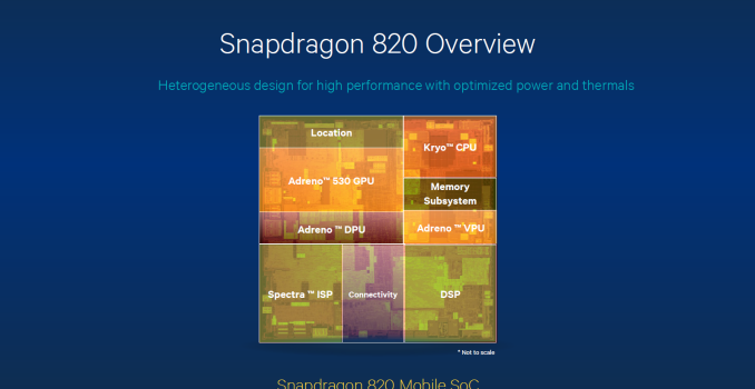
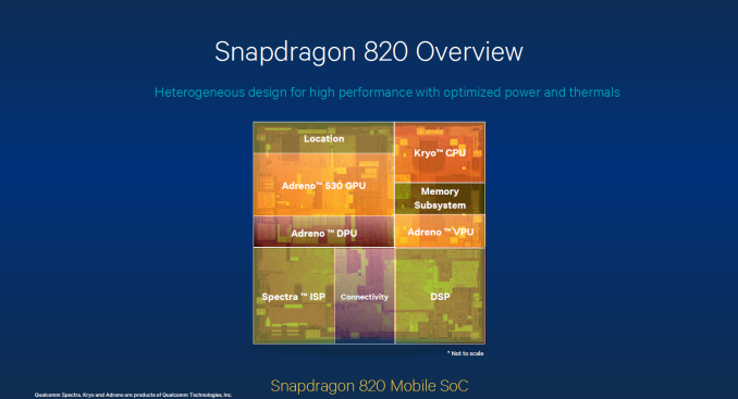
Snapdragon 820 is still a mystery as far as official information from Qualcomm goes. However, today Qualcomm has given a bit of insight into their upcoming SoC. While there’s still no information about the CPU portion featuring Qualcomm’s custom 64-bit cores known as ‘Kryo’, there are some details about the Adreno 510 and 530 GPUs, as well as Qualcomm’s Spectra image signal processor.

Because Adreno 530 is their new flagship GPU, Qualcomm’s press release focuses more on the 530 than the 510. The performance figures released by Qualcomm describe Adreno 530 as being 40% faster than Adreno 430 on average, while also consuming 40% less power. This result is described as an average of “the top graphics benchmarks”, and while it’s still generally a good idea to take vendor provided numbers with a grain of salt, if the power and performance gains over Adreno 430 are anywhere in the ballpark of Qualcomm’s 40% figure then Adreno 530 should end up being quite impressive.

On the API side, Adreno 500 series GPUs will support OpenGL ES 3.1 + AEP (Android Extension Pack), Renderscript, Vulkan, and OpenCL 2.0. With OpenCL 2.0 comes support for Shared Virtual Memory (SVP), which allows an OpenCL host program and a device’s kernel to share a virtual address space so access to data structures like lists and trees can be easily shared between the host and GPU. Adreno 530 has varying improvements to GPGPU performance when compared to Adreno 430, but Qualcomm’s slides show video processing as demonstrating the greatest improvement with a 2.5x increase in compute performance. This is also the area where efficiency gains for generational improvements typically happen, so we expect fixed-function codec support although this information is not yet provided.

As for the ISP, it’s still the case that mobile image signal processors are black boxes. Qualcomm is stating that their Spectra ISP in Snapdragon 820 will be able to support 3 simultaneous cameras at up to 25MP and at 30fps with no shutter lag. The Spectra ISP will also use MIPI’s higher bandwidth C-PHY serial interface, which supports the enhanced camera support. As well as this, new developer and user-facing features include support and APIs for depth maps and using dual cameras to perform refocusing or other visual effects – because Qualcomm is just the SoC manufacturer, it is up to the smartphone OEMs to implement dual-camera/depth-maps as a feature as well.

According to Qualcomm, Snapdragon 820 will start showing up in devices during the first half of 2016. Hopefully between now and then there’s more information from Qualcomm about the other aspects of their new SoC, including their Kryo custom CPU core. In Q1 we will be at Mobile World Congress, so we may see more information at that time.

Source: Qualcomm, slides via Slashgear

Qualcomm Details the Adreno 530 GPU and ISP inside the Snapdragon 820

Qualcomm Details the Adreno 530 GPU and ISP inside the Snapdragon 820

Snapdragon 820 is still a mystery as far as official information from Qualcomm goes. However, today Qualcomm has given a bit of insight into their upcoming SoC. While there’s still no information about the CPU portion featuring Qualcomm’s custom 64-bit cores known as ‘Kryo’, there are some details about the Adreno 510 and 530 GPUs, as well as Qualcomm’s Spectra image signal processor.

Because Adreno 530 is their new flagship GPU, Qualcomm’s press release focuses more on the 530 than the 510. The performance figures released by Qualcomm describe Adreno 530 as being 40% faster than Adreno 430 on average, while also consuming 40% less power. This result is described as an average of “the top graphics benchmarks”, and while it’s still generally a good idea to take vendor provided numbers with a grain of salt, if the power and performance gains over Adreno 430 are anywhere in the ballpark of Qualcomm’s 40% figure then Adreno 530 should end up being quite impressive.

On the API side, Adreno 500 series GPUs will support OpenGL ES 3.1 + AEP (Android Extension Pack), Renderscript, Vulkan, and OpenCL 2.0. With OpenCL 2.0 comes support for Shared Virtual Memory (SVP), which allows an OpenCL host program and a device’s kernel to share a virtual address space so access to data structures like lists and trees can be easily shared between the host and GPU. Adreno 530 has varying improvements to GPGPU performance when compared to Adreno 430, but Qualcomm’s slides show video processing as demonstrating the greatest improvement with a 2.5x increase in compute performance. This is also the area where efficiency gains for generational improvements typically happen, so we expect fixed-function codec support although this information is not yet provided.

As for the ISP, it’s still the case that mobile image signal processors are black boxes. Qualcomm is stating that their Spectra ISP in Snapdragon 820 will be able to support 3 simultaneous cameras at up to 25MP and at 30fps with no shutter lag. The Spectra ISP will also use MIPI’s higher bandwidth C-PHY serial interface, which supports the enhanced camera support. As well as this, new developer and user-facing features include support and APIs for depth maps and using dual cameras to perform refocusing or other visual effects – because Qualcomm is just the SoC manufacturer, it is up to the smartphone OEMs to implement dual-camera/depth-maps as a feature as well.

According to Qualcomm, Snapdragon 820 will start showing up in devices during the first half of 2016. Hopefully between now and then there’s more information from Qualcomm about the other aspects of their new SoC, including their Kryo custom CPU core. In Q1 we will be at Mobile World Congress, so we may see more information at that time.

Source: Qualcomm, slides via Slashgear