CPUs


Intel's 10nm Briefly Appears: Dual Core Cannon Lake in Official Documents

Intel’s 10nm Briefly Appears: Dual Core Cannon Lake in Official Documents

Intel briefly listed two 10nm Cannon Lake processors in a microcode update document this week, confirming that it has shipped such chips, although we expect it to be in small quantities. Intel has since removed the references to them from the public version of the paper.

Intel has adjusted its 10nm roadmap multiple times in the recent years. Back in 2013, the company planned to make CPUs produced using its 10nm technology available in 2015. Then, the company pushed them to 2016, but that was a minor change. In mid-2015 the chipmaker delayed its 10 nm products to late 2017. Then in early-2016, Intel switched its “Tick-Tock” cadence to “Process-Architecture-Optimization” model, officially prolonging lifecycles of its manufacturing technology nodes and changing its approach to new product development in general. When it comes to 10 nm products, Intel has not made formal announcements about any product family yet, but said earlier this year in a side-presentation to its CES keynote that it had shipped some of them to customers in 2017.

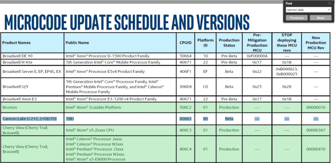
Since the company did not disclose any details about the 10nm CPUs it shipped, it naturally caused further questions on the state of Intel’s 10nm process in general and when the Cannon Lake products, expected to be the first on 10nm, were coming. Fortunately, our friends at Tom’s Hardware noticed Cannon Lake processors in the latest version of Intel’s microcode update document earlier this week. After the fact, Intel has since removed the references from the document.

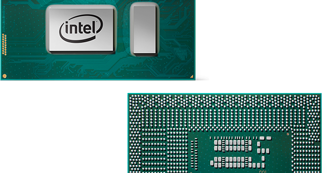
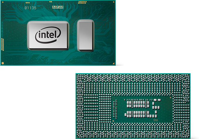
The first version of the document, as it appears, suggests that Intel has shipped Cannon Lake-U CPUs in 2+2 and 2+0 configurations to undisclosed customers. The “2+2” denotes that a chip has two processing cores (the first number) as well as GT2-class graphics (the second number), whereas the “2+0” indicates that a dual-core chip has no iGPU at all. Intel’s “U” series parts, aimed at the 15W notebook market, usually feature an integrated chipset in the CPU package. Therefore, the CNL-U 2+2 and CNL-U 2+0 parts are aimed primarily at mobile and low-power applications.

It is noteworthy that in the recent years Intel has begun commercial roll-outs of its new CPUs starting with ultra-low-power 4.5W Y-series processors, e.g., Broadwell-Y in 2014, Skylake-Y in 2015, and Kaby Lake-Y in 2016. If Intel is launching its U-series chips with a TDP of 15 W first for 10nm, this would indicate a change in policy. So it is surprising to see that Intel has started shipments of Cannon Lake-U, but not Cannon Lake-Y.

A natural question that arises because of the listing is whether Intel has started to ship its CNL-U parts in mass quantities to PC makers. Intel has not disclosed where these parts have been sold, which could be for entry-level low-power laptops, or to certain specific customers and requests with custom/semi-custom CNL products. While a CNL-U 2+2 CPU could be used for inexpensive notebooks, a CNL 2+0 part would fit into applications that either do not require a display controller at all (such as routers, NAS, DAS, etc.), or can use a discrete GPU (a low-end PC with a low-end/outdated dGPU – there are a lot of such machines sold in developing countries, a system for software/hardware development/compatibility tests/etc.). Unfortunately, at this point it is completely unclear where Intel has shipped these 10nm parts. 

Related Reading

Intel Adds Mobile Core i3-8130U to Lineup: Increased Cache and Turbo

Intel Adds Mobile Core i3-8130U to Lineup: Increased Cache and Turbo

Intel on Tuesday introduced the Core i3-8130U, its first mobile 8th Generation Core i3 processor. The new chip features two cores operating at a high frequency and supports Turbo Boost 2.0 technology to make them even faster when power and temperatures permit. The CPU also gains an L3 cache size increase over its predecessors, stepping up to 2MB of inclusive L3 cache per core. However, the new processor is listed as only $16 cheaper than one above it in Intel’s stack, the quad-core Core i5-8250U, posing questions about its appeal to the end-user.

The Core i3-8130U

The Intel Core i3-8130U has two cores with Hyper-Threading, operating at 2.2 GHz base frequency and speeding up to 3.4 GHz in Turbo Boost 2.0 mode; the chip is outfitted with 4 MB of L3 cache and has a 15 W TDP. Previous-generation mobile ULV Core i3 processors came with 3 MB of L3 cache and did not feature Turbo mode, by comparison. The addition of Turbo comes at a different cost, as it would appear that Intel has reduced the base frequency to compensate: the default frequency of the previous generation Core i3-7130U was 2.7 GHz, whereas the new Core i3-8130 is at 2.2 GHz. There is also the added complication that Turbo frequency boosting depends on multiple factors, such as chassis design and cooling performance.

When it comes to graphics and memory, the new CPU features the UHD Graphics 620 iGPU (GT2) as well as a dual-channel memory controller supporting LPDDR3-2133 or DDR4-2400. From silicon point of view, we are dealing with a Kaby Lake Refresh 2+2 design, and the main difference with the original Kaby Lake is the addition of native support of HDMI 2.0, HDCP 2.2, and possible minor fixes.

Intel Mobile Core i3 and Core i5 Processors
  Core i5-8250U Core i3-8130U Core i3-7130U
CPU Cores/Threads 4/8 2/4
Frequency Base 1.6 GHz 2.2 GHz 2.7 GHz
Dual-Core Turbo ? 3.4 GHz 2.7 GHz
Single-Core Turbo 3.4 GHz 3.4 GHz 2.7 GHz
TDP (PL1) @ Base Frequency 15 W
Instantaneous Turbo Power (PL2) 44 W ? 19 W
Configurable TDP-up Freq. 1.8 GHz
Configurable TDP-up 25 W
L3 Cache 6 MB 4 MB 3 MB
Graphics GPU UHD 620 HD 620
EUs 24 EUs
Base Freq. 300 MHz
Turbo Freq. 1.1 GHz 1 GHz
DRAM Support LPDDR3-2133
DDR4-2400
128-bit
DDR3L-1600
LPDDR3-1866
DDR4-2133
128-bit
Price at Launch $297 $281 $281
Launch Timeframe Q3 2017 Q1 2018 Q2 2017

Intel positions the Core i3-8130U as its lowest-cost offering for the latest mainstream notebooks and 2-in-1 PCs. The processor is listed at $281 in 1000-unit quantities, which is only $16 cheaper than the price of the quad-core Core i5-8250U. Historically, RCPs of Intel’s higher-end mobile Core i3 products have matched (or almost matched) prices of the company’s entry mobile Core i5 offerings, so there is nothing new here.

However, the difference between 7th Generation mobile Core i3 and Core i5 was negligible and pricing of these CPUs just reflected that. By contrast, today we are dealing with a $297 quad-core Core i5-8250U operating at 1.6-3.4 GHz as well as a $281 dual-core Core i3-8130U operating at 2.2-3.4 GHz. Despite the clock speed difference, we would expect many modern workloads that are multi-threaded to give the i5-8250U a significant advantage over the i3-8130U.  In any case, at $281, the new CPU is currently the most affordable 8th Generation mobile Core processor and it will enable PC makers to build slightly cheaper versions of their latest laptops or 2-in-1s. 

Note: The image above depicts Intel’s 8th Generation Core i7 SoC. The 8th Generation Core i3 SoC may look differently.

Related Reading

AMD Readies Ryzen 3 2200GE & Ryzen 5 2400GE APUs with Reduced TDP

AMD Readies Ryzen 3 2200GE & Ryzen 5 2400GE APUs with Reduced TDP

AMD is preparing to release low-power versions of its Ryzen APUs with built-in Radeon Vega graphics. The new Ryzen 3 2200GE and Ryzen 5 2400GE chips will have a 35 W TDP and will operate at lower frequencies when compared to the Ryzen 3 2200G and the …

AM4 Motherboard BIOS Updates Released to Support AMD Ryzen APUs

AM4 Motherboard BIOS Updates Released to Support AMD Ryzen APUs

AMD’s Ryzen CPUs made a large impact on the market starting around mid-2017 when they were released. When Ryzen based CPUs hit the scene, performance was on generally on par or better than its Intel counterparts and pricing was notably better for the same thread count. This was a dramatic change from previous generations and brought competition back to the CPU market. Fast forward to today and AMD’s new Ryzen-based APUs are being released – the Raven Ridge-based Ryzen 5 2400G and Ryzen 3 2200G – which merge AMD’s Vega GPU architecture along with Ryzen CPU. 

With this latest release of what AMD is calling their 2000-series processors, existing X370, B350, and A320 based motherboards will require a BIOS update for proper support of the new APUs. As a result, all of the major board partners have released updates for their respective lineups to include AMD’s AGESA 1.1.0.1 microcode, allowing existing boards to fully support these new APUs.

In accordance with this latest round of updates, we have compiled a list from four major OEMs of all the updated BIOS versions below. Missing is Biostar who did not make any announcements. We checked the website and as of today, they have not released new BIOSes for their AM4 boards which include the AGESA 1.1.0.1 update supporting these APUs. 

EDITOR’S NOTE: Biostar announced its support list 2/12 after publication. It has been added below.


MSI

MSI distributed a press release a couple days ago on its website. These can be found at the motherboard’s site and the support section.

MSI X370 Motherboards
Name PCB Version BIOS Version
X370 XPower Gaming Titanium 1.1 E731AMS.1C0
X370 Gaming M7 ACK 1.1 E7A35AMS.150
X370 Gaming Pro Carbon AC 1.1 E7A32AMS.280
X370 Gaming Pro Carbon 1.1 E732AMS.1C0
X370 Krait Gaming 1.0 / 1.1 E7A33AMS.190
X370 Gaming Pro 2.0 / 2.1 E733AMS.480
X370 SLI Plus 2.0 / 2.1 E7A33AMS.390
X370 Gaming Plus 3.0 E7A33AMS.580
B350
B350 Gaming Pro Carbon 1.1 E7B00AMS.190
B350 Krait Gaming 1.0 E7B08AMS.180
B350 Tomahawk Plus 1.2 E7B36AMS.180
B350 Tomahawk 1.0 E7A34AMS.1C0
B350 Tomahawk Arctic 3.0 E7A34AMS.HA0
B350 Gaming Plus 4.0 E7A34AMS.M70
B350M Mortar 1.1 E7A37AMS.1B0
B350M Mortar Arctic 2.1 E7A7AMS.AA0
B350M Bazooka 1.0 E7A38AMS.1A0
B350M Gaming Pro 1.0 E7A39AMS.2C0
B350 PC Mate 2.0 E7A34AMS.AA0
B350M Pro-VD Plus 1.1 E7B38AMS.250
B350M Pro-VDH 2.0 E7A38AMS.A90
B350I-S01 1.1 E7A40AMS.230
B350I Pro AC 1.1 E7A40AMS.110
B350M Pro-VH Plus 1.0 E7B07AMS.250
A320
A320M Gaming Pro 1.0 E7A39AMS.190
A320M Bazooka 1.0 E7A38AMS.280
A320M Grenade 3.0 E7A39AMS.A80
A320M Pro-VD/S 1.0 E7A36AMS.270
A320M Pro-VH Plus 1.0 E7B07AMS.360
A320M Pro-VHL 1.0 E7B07AMS.160
A320M Pro-VD Plus 1.0 E7B38AMS.310
A320M Pro-VD Plus 1.1 E7B38MAS.150


Asus

Asus also sent out an official announcement on their new BIOSes. The Asus website lists them as well as instructions on how to update. The X370 Crosshair motherboards are able to flash via BIOS Flashback or EX Flash 3 while the rest of the of the boards will use the more traditional EX Flash 3. 

Asus X370 Motherboards
Name BIOS Version
ROG Crosshair VI Extreme 3502
ROG Crosshair VI Hero (Wi-Fi AC) 3502
ROG Crosshair VI Hero 3502
ROG Strix X370-F Gaming 3803
ROG Strix X370-I Gaming 3803
Prime X370-Pro 3803
Prime X370-A 3803
B350
ROG Strix B350-F Gaming 3803
ROG Strix B350-I Gaming 3803
TUF B350M-Plus Gaming 3803
Prime B350-Plus 3803
Prime B350M-A 3803
Prime B350M-E 3803
Prime B350M-K 3803
B350M-Dragon 3803
A320
Prime A320M-C  R2.0 3803
Prime A320M-A 3803
Prime A320M-E 3803
Prime A320M-K 3803
EX-A320M-Gaming 3803


ASRock

ASRock also made an announcement, however, it was only on their Japanese website or via email to the press. Since that was published, additional BIOSes have already been released and are listed below.

ASRock X370 Motherboards
Name BIOS Version
X370 Taichi 4.40
X370 Killer SLI/AC 4.50
X370 Killer SLI 4.50
Fatal1ty X370 Professional Gaming 4.40
Fatal1ty X370 Gaming K4 4.50
Fatal1ty X370 Gaming X 4.50
Fatal1ty X270 Gaming-ITX/AC 4.40
B350
AB350 Pro4 4.50
AB350M Pro4 4.50
AB350M 4.40
AB350M-HDV 4.40
Fatal1ty AB350 Gaming-ITX/AC 4.40
Fatal1ty AB350 Gaming K4 4.60
A320
A320M Pro4 4.50
A320M 4.40
A320M-DGS 4.40
A320M-HDV 4.40


GIGABYTE

GIGABYTE did not have an official announcement but are listed on the website for all AM4 motherboards. 

GIGABYTE X370 Motherboards
Name BIOS Version
GA-AX370M-Gaming 3 F20
GA-AX370M-DS3H F20
GA-AX370-Gaming K7 F20
GA-AX370-Gaming K5 F20
GA-AX370-Gaming K3 F20
GA-AX370-Gaming 5 F20
GA-AX370-Gaming 3 F20
GA-AX370-Gaming F20
B350
GA-AB350M-Gaming 3 F20
GA-AB350N-Gaming WiFi T20h
GA-AB350M-DS3H F20
GA-AB350M-D3V F20
GA-AB350M-HD3 F20
GA-AB350M-DS2 F20
GA-AB350-D3H F20
GA-AB350-Gaming 3 F20
GA-AB350-Gaming F20
A320
GA-A320M-S2H F20
GA-A320MA-M.2 F20
GA-A320M-D2P F20
GA-A320M-DS2 F20
GA-A320M-HD2 F20
GA-A320-DS3 F20


Biostar

Biostar announced their support through the Taiwan website

Biostar X370 Motherboards
Name BIOS Version
Racing X370GT7 F12
Racing X370GT5 F12
Racing X370GT3 F12
Racing X370GTN F12
B350
Racing B350GT5 F12
Racing B350GT3 F12
Racing B350GTN F12
Racing B250ET2 F12
TB350-BTC F12
A320
TA320-BTC F12
A320MH Pro F12
A320MD Pro F12

Related Reading:

Marrying Vega and Zen: The AMD Ryzen 5 2400G Review

AMD’s new launch of APUs hits the apex of the 2017 designs that tend the balance sheet black. After a return to high performance on x86 with the Ryzen CPU product line, and the ‘we can’t product enough’ Vega graphics, AMD has inserted several product lines that combine the two. Today is the launch of the desktop socket edition APUs, with four Zen cores and up to 11 Vega compute units. AMD has historically been aggressive in the low-end desktop space, effectively killing the sub-$100 discrete graphics market. The new APUs now set the bar even higher. In this review we focus on the Ryzen 5 2400G, but also test the Ryzen 3 2200G.