GPUs


AMD Quietly Releases Radeon R9 370X, China-Only For Now

AMD Quietly Releases Radeon R9 370X, China-Only For Now

Back in June when AMD launched the Radeon 300 series, AMD made the unusual move of only releasing refresh SKUs for around half of their products. While the 390 series saw the release of the vanilla 390 and 390X parts, the 380, 370, and 360 were all released with just one SKU respectively. Furthermore all three parts were the second-tier configurations for their respective GPUs, each packing a partially disabled GPU. At the time we suspected that AMD was simply holding back some SKUs to avoid flooding the market all at once and to release those SKUs at a more convenient opportunity, and it looks like this is indeed the case.

Alongside yesterday’s R9 Nano unveil, AMD also quietly launched the R9 370X. The unexpectedly quiet launch of the SKU is due to the fact that AMD is only releasing it on a regional basis, at least for the time being. As reported by PCWorld, who received confirmation from AMD, the R9 370X is only going to be available in China at this time.

The China-only launch of the R9 370X comes shortly after the launch of NVIDIA’s GeForce GTX 950, a card that we expect will be especially popular in China given pricing, economics, and the specific popularity of free-to-play games in that market. As a result, AMD releasing a China-only SKU, while not normal, is not without merit since it’s likely going to be China and the greater APAC region where the real fight over sales volume for this class of parts will be. Still, we also expect that R9 370X will eventually come to North America, similar to how AMD rolled out some of the 200 series SKUs.

AMD GPU Specification Comparison
  AMD Radeon R9 370X AMD Radeon R7 370 AMD Radeon R9 270X AMD Radeon HD 7870
Stream Processors 1280 1024 1280 1280
Texture Units 80 64 80 80
ROPs 32 32 32 32
Core Clock ? 925MHz 1000MHz 1000MHz
Boost Clock ? 975MHz 1050MHz N/A
Memory Clock 5.6Gbps GDDR5 5.6Gbps GDDR5 5.6Gbps GDDR5 4.8Gbps GDDR5
Memory Bus Width 256-bit 256-bit 256-bit 256-bit
VRAM 2GB/4GB 2GB 2GB 2GB
FP64 1/16 1/16 1/16 1/16
TrueAudio N N N N
Transistor Count 2.8B 2.8B 2.8B 2.8B
Typical Board Power ? 110W 180W 190W
Manufacturing Process TSMC 28nm TSMC 28nm TSMC 28nm TSMC 28nm
Architecture GCN 1.0 GCN 1.0 GCN 1.0 GCN 1.0
GPU Pitcairn Pitcairn Pitcairn Pitcairn
Launch Date China-Only 06/18/15 10/08/13 03/05/12
Launch Price N/A $149 $199 $349

As for the R9 370X itself, the SKU is the refresh successor to the R9 270X. This means we’re looking at a fully-enabled Pitcairn GPU with all 1280 stream processors enabled. This marks the fourth such desktop SKU for the full Pitcairn configuration, following the original Radeon HD 7870 and the R9 270 & 270X, both of the latter being fully enabled parts.

AMD Radeon Product Evolution
Predecessor GPU Successor
Radeon R9 290X Hawaii Radeon R9 390X
Radeon R9 285 Tonga Radeon R9 380
Radeon R9 270/270X
Radeon HD 7870
Pitcairn Radeon R9 370X
Radeon R7 265
Radeon HD 7850
Radeon R7 370
Radeon R9 260 Bonaire Radeon R9 360

At this time we don’t have official AMD specifications for the R9 370X SKU (nor do we expect to get them). Furthermore based on information released by TechPowerUp, the first card released is a factory overclocked Sapphire model, so we have limited information available on clockspeeds. However based on the 5.6Gbps memory speed, it would appear that this is closer to a straight re-badge than was the case with the release of the 200 series, as AMD reworked their board designs to improve memory clockspeeds for that refresh.


Sapphire’s R9 370X Vapor X (Image Courtesy TechPowerUp)

In any case, while the R9 370X is China-only for the time being, don’t be too surprised if we see it released in North America before too long, especially once R9 270 series supplies start dropping.

Sources: TechPowerUp & PCWorld

AMD Announces Radeon R9 Nano; mini-ITX Card Shipping September 10th

AMD Announces Radeon R9 Nano; mini-ITX Card Shipping September 10th

Back in June at AMD’s R9 Fury X/Fiji GPU launch event, the company unveiled that there would be four products based on Fiji. Fury X and Fury – which have since launched – and then two additional products, the R9 Nano and a yet-to-be-named dual-GPU card. Uncharacteristicly for AMD, the R9 Nano was unveiled some time before it would ship in order to demonstrate some of the size benefits of the Fiji GPU and its HBM, with the card initially receiving a tentative launch date of “summer”.

Now with August coming to a close, AMD is formally announcing the R9 Nano ahead of its full launch next month. The card, which will be AMD’s take on a premium, specialty product for the mini-ITX market, will be hitting retailer shelves on September 10th for $649.

AMD GPU Specification Comparison
  AMD Radeon R9 Fury X AMD Radeon R9 Fury AMD Radeon R9 Nano AMD Radeon R9 390X
Stream Processors 4096 3584 4096 2816
Texture Units 256 224 256 176
ROPs 64 64 64 64
Boost Clock 1050MHz 1000MHz 1000MHz 1050MHz
Memory Clock 1Gbps HBM 1Gbps HBM 1Gbps HBM 6Gbps GDDR5
Memory Bus Width 4096-bit 4096-bit 4096-bit 512-bit
VRAM 4GB 4GB 4GB 8GB
FP64 1/16 1/16 1/16 1/8
TrueAudio Y Y Y Y
Transistor Count 8.9B 8.9B 8.9B 6.2B
Typical Board Power 275W 275W 175W 275W
Manufacturing Process TSMC 28nm TSMC 28nm TSMC 28nm TSMC 28nm
Architecture GCN 1.2 GCN 1.2 GCN 1.2 GCN 1.1
GPU Fiji Fiji Fiji Hawaii
Launch Date 06/24/15 07/14/15 09/10/15 06/18/15
Launch Price $649 $549 $649 $429

Diving right into the design and specs, the R9 Nano is designed to be a showcase piece for the space savings that HBM technology offers. With Fiji’s 4GB of VRAM confined to a quartet of small, stacked packages near the GPU die, the overall space occupied by the complete GPU package is quite small, just over 1000mm2. Similar to what we saw with the R9 Fury X, the lack of large GDDR5 memory chips allows AMD to build a smaller board overall, and R9 Nano is to be the logical extension of what R9 Fury X started, bringing Fiji down to a mini-ITX sized video card.

In order to achieve this AMD has turned to a combination of chip binning and power reductions to make a Fiji card viable as the desired size. The Fiji GPUs going into the R9 Nano will be AMD’s best Fiji chips (from a power standpoint), which are fully enabled Fiji chips that have been binned specifically for their low power usage. Going hand in hand with that, AMD has designed the supporting power delivery circuitry for the R9 Nano for just 175W, allowing the company to further cut down on the amount of space required for the card.

The end result is that from a specification standpoint the R9 Nano should be an impressive, tiny terror. Since it’s a full Fiji GPU the R9 Nano doesn’t take an immediate hit to its performance relative to the R9 Fury X, featuring the same 4096 stream processors and 4096-bit ultra-wide HBM memory bus. The only real differences between R9 Fury X and R9 Nano are the clockspeed and the TDP/power targets. The R9 Nano will ship with a boost clock of 1000MHz versus R9 Fury X’s 1050MHz boost clock, and the TDP is 175W versus 275W.

The resulting performance difference in turn will come down to power limits. While R9 Nano has a 1000MHz boost clock, even with AMD’s binning 175W is a relatively harsh power limit for such a powerful GPU, and consequently the R9 Fury X the R9 Nano is expected to power throttle under normal circumstances. AMD tells us that the typical gaming clock will be around the 900MHz range, with the precise value depending on the power requirements of the workload being run. As to why AMD is shipping the card at 1000MHz even when they don’t expect it to be able to sustain the clockspeed under most games, AMD tells us that the higher boost clock essentially ensures that the R9 Nano is only ever power limited, and isn’t unnecessarily held back in light workloads where it could support higher clockspeeds.

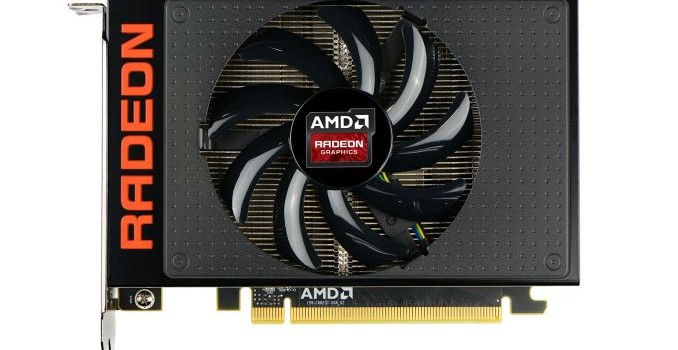
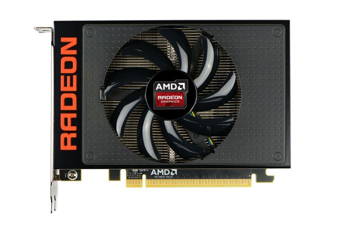
Moving on, the physical board itself measures just 6” long, allowing the complete card to fit within the full width of a mini-ITX motherboard. Power delivery is handled by a single 8-pin PCIe power socket, which is becoming increasingly common, replacing the 2x 6-pin setup for 150W-225W cards. In order to get the length of the board down AMD has moved some of the power delivery circuitry to the back of the card; the front of the card still contains the inductors and heat-sensitive MOSFETs, while a number of capacitors are on the rear of the card (and is why you won’t find a backplate).

Responsibility for cooling the card falls to the R9 Nano’s new open air cooler, an aggressive design that has been specifically tailored to allow the card to effectively dissipate 175W of heat in such a small space. The overall design is best described as a combination open-air and half-blower hybrid; the design is technically open-air, however with only a single fan AMD has been able to align the heatsink fins horizontally and then place the fan in the center of the heatsink. The end result is that roughly half of the heat produced by the card is vented outside of the case, similar to a full blower, while the other half of the heat is vented back into the case. This reduces (though doesn’t eliminate) the amount of hot air being recycled by the card.

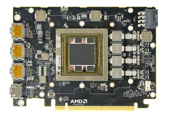
Drilling down, we find that the R9 Nano’s heatsink assembly is actually composed of two separate pieces. The primary heatsink is a combination vapor chamber and heatpipe design. A copper vapor chamber serves to draw heat away from the Fiji GPU and HBM stacks, and then heatpipes are used to better distribute heat to the rest of the heatsink. Meanwhile a small secondary heatsink with its own heatpipe is mounted towards the rear of the card and is solely responsible for cooling the MOSFETs.

The use of a vapor chamber in the R9 Nano makes a lot of sense given the fact that vapor chambers are traditionally the most efficient heatsink base type, however the R9 Nano is also unique in that we typically don’t see vapor chambers and heatpipes used together. Other designs such as the high-end GeForce series use a single large vapor chamber across the entire heatsink base, so among reference cards at least the R9 Nano stands alone in this respect, and it will be interesting to see what cooling performance is like.

That said, AMD is rather confident in their design and tells us that the R9 Nano should never thermally throttle; the card’s thermal throttle point is 85C, meanwhile the card is designed to operate at around 75C, 10C below the throttling point. Similarly, AMD is promising that R9 Nano will also be a quiet card, though as this is far more relative we’ll have to see how it does in testing.

From a marketing standpoint, AMD will be spending a fair bit of time comparing the R9 Nano to the reference R9 290X, AMD’s former flagship Hawaii card. The reference R9 290 cards were something of a low point for AMD in terms of cooling efficiency and noise, so they are eager to present the R9 Nano as an example of how they have learned from their earlier mistakes. Going up against what is admittedly a low bar, AMD is telling us that the R9 Nano is 30% faster than the R9 290X, draws 30% less power than the R9 290X, and is much, much quieter than their former flagship. Thanks in large part to the combination of Fiji’s architectural improvements and AMD’s aggressive binning, the R9 Nano should offer around 2x the energy efficiency of the R9 290X, and of course it will be a much smaller card as well.

Otherwise against AMD’s Fury lineup, the performance of the R9 Nano will potentially be rather close. If AMD’s 900MHz average clockspeed figure proves to be correct, then the R9 Nano would deliver around 85% of the R9 Fury X’s performance, or around 92% of the R9 Fury’s. This would make it slower than either of the existing Fiji cards, but somewhere near (and likely ahead of) the R9 390X.

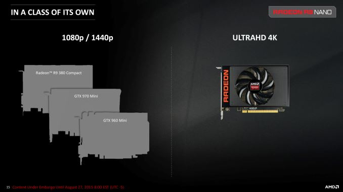
More importantly for AMD though, the R9 Nano should easily be the most powerful mini-ITX card on the market. The other major mini-ITX cards are based on smaller, less powerful video cards such as the Radeon R9 280 (Tonga) and GeForce GTX 970 (GM204), both of which a 900MHz Fiji will easily clear. By how much is going to depend on a few factors, including the actual average gaming clockspeeds and the games in question, but overall in the mini-ITX space there’s every reason to expect that R9 Nano will stand at the top.

Which brings us to the final aspect of the R9 Nano, which is pricing and positioning. For the R9 Nano AMD is going to positioning the card as a luxury product, similar to NVIDIA’s Titan series, which is to say that it will offer unparalleled performance for the segment of the market it’s designed for – in this case mini-ITX – but it will also fetch a higher price as a result. In the case of the R9 Nano, this means $650.

From a silicon lottery standpoint R9 Nano will feature AMD’s best Fiji chips, and the vapor chamber cooler, though not quite as intricate as R9 Fury X’s CLLC, is still an advanced cooler with a higher cost to go with it. As a result it’s unsurprising that AMD is seeking to charge a premium for the product, both to cover the higher costs and to take advantage of their expected performance lead within the mini-ITX market. Practically speaking the mini-ITX market is a small one relative to the larger gaming PC market (pun intended), and while there is some overlap with the power efficient gaming PC market, it’s hard to say just how much overlap there is. Regardless, AMD’s pricing and messaging make it clear that the R9 Fury series is intended to be AMD’s top performance cards and price/performance kingpins, while R9 Nano is a specialty card for a smaller market that’s currently underserved.

Of course there’s also going to be the question of how many cards AMD can even supply. Binning means that only a fraction of Fiji chips will ever make the cut, so R9 Nano is never going to be a high volume part along the lines of the R9 Fury series. What remains to be seen then is how much of a market exists for $650 mini-ITX cards, and then if AMD can supply enough cards for that market. Though given AMD’s unique situation, I don’t doubt that they’ll be able to sell a number of these cards.

On that note, we’re hearing that the overall Fiji supply situation is looking up. R9 Fury series cards have been in short supply in the US since the June/July launches, with card supplies improving just within the last couple of weeks. For the R9 Nano launch AMD has been stockpiling cards for the initial rush of sales, and beyond that we’ll have to see what becomes of the supply situation.

Finally, once the supply situation does improve AMD tells us that we may see some custom R9 Nano cards come later in Q4 of this year. AMD has been very vague on this point, but from what they’re telling us they’re going to be letting partners take a shot at developing Nano designs of their own. So while the launch on September 10th and for the next couple of months after that will be pure reference, we may see some custom designs by the end of the year.

And with that we end for now. Please be sure to check back in on September 10th for our full review of the smallest member of AMD’s Fiji family.

Summer 2015 GPU Pricing Comparison
AMD Price NVIDIA
Radeon R9 Fury X
Radeon R9 Nano
$649 GeForce GTX 980 Ti
Radeon R9 Fury $549  
  $499 GeForce GTX 980
Radeon R9 390X $429  
Radeon R9 390 $329 GeForce GTX 970
NVIDIA Launches GeForce GTX 950; GM206 The Lesser For $159

NVIDIA Launches GeForce GTX 950; GM206 The Lesser For $159

It still doesn’t seem like it was all that long ago, but at this point it was 18 months ago when NVIDIA launched the first member of their Maxwell 1 GPU family, the GM107-based GeForce GTX 750 series. A prelude of things to come, the GTX 750 series introduced us to NVIDIA’s highly optimized Maxwell architecture, reaching new levels of energy efficiency and also work efficiency per CUDA core. What the Maxwell 1 architecture lacked that Maxwell 2 brought with us later in 2014 was support for newer features such as HDMI 2.0 and graphical features like conservative rasterization – Maxwell 1 from a feature perspective was closer to a highly power optimized Kepler in that regard.

Maxwell 1 of course was relatively short-lived before NVIDIA moved on to Maxwell 2, delivering GM204, GM206, and GM200 over the last 12 months. Given NVIDIA’s unusual rollout of Maxwell 1 and Maxwell 2, there has always been some question of if and how NVIDIA would follow up on GM107; it’s a power efficient architecture, but there’s a real feature disparity. As has become clear since then, NVIDIA is not going to rev another lower-end GPU so soon after the last one. Instead, with GM206 currently powering only a single product – GTX 960 – NVIDIA is instead going to cut down GM206 to close the gap in as reasonable a manner as the situation allows.

The end result of that is that today NVIDIA is launching the GeForce GTX 950, the Maxwell 2 update for much of the rest of NVIDIA’s lineup. As yet another GM206 SKU there are no big surprises here – we’re already familiar with GM206 – but this brings GM206’s performance and features down to a lower price point of $159.

Meanwhile on a quick housekeeping note, as today’s launch comes at the tail end of Intel’s IDF 2015, timing constraints mean that we won’t be posting our review of the GTX 950 today. Our full review will be up next week once the show has concluded, so be sure to check back a bit later this month.

NVIDIA GPU Specification Comparison
  GTX 960 GTX 950 GTX 750 Ti GTX 650 Ti
CUDA Cores 1024 768 640 768
Texture Units 64 48 40 64
ROPs 32 32 16 16
Core Clock 1126MHz 1024MHz 1020MHz 925MHz
Boost Clock 1178MHz 1188MHz 1085MHz N/A
Memory Clock 7GHz GDDR5 6.6GHz GDDR5 5.4GHz GDDR5 5.4GHz GDDR5
Memory Bus Width 128-bit 128-bit 128-bit 128-bit
VRAM 2GB 2GB 2GB 1GB
FP64 1/32 FP32 1/32 FP32 1/32 FP32 1/24 FP32
TDP 120W 90W 60W 110W
Architecture Maxwell 2 Maxwell 2 Maxwell 1 Kepler
GPU GM206 GM206 GM107 GK106
Transistor Count 2.94B 2.94B 1.87B 2.54B
Manufacturing Process TSMC 28nm TSMC 28nm TSMC 28nm TSMC 28nm
Launch Date 01/22/15 08/20/15 02/18/14 10/09/12
Launch Price $199 $159 $149 $149

Diving into the specifications, NVIDIA has cut down GM206 in such a manner that I suspect it’s not quite as steep a cut from GTX 960 as some readers would have expected. Compared to GTX 960, GTX 950 loses one-quarter of its SMMs – going from 8 to 6 – bringing the CUDA core count down from 1024 to 768. Otherwise the memory bus/ROP clusters are left intact, with 32 ROPs connected to a 128-bit GDDR5 memory bus.

As for clockspeeds, relative to GTX 960 what we’re seeing both is and isn’t much of a cut. GTX 950 ships with a much wider delta between the base clock and boost clock than GTX 960, with a 1024MHz base and 1188MHz boost. This larger disparity is for power reasons, as a lower base clock goes hand-in-hand with tighter TDP restrictions (more on this in a sec). What this means is that GTX 950 can boost almost as high as GTX 960, but when facing a more strenuous workload it will have to back off in a manner GTX 960 did not. Meanwhile memory clockspeeds have also taken a haircut from 7GHz to 6.6GHz. This mostly seems to be for the purpose of creating an artificial distinction, as no one supplies a 6.6GHz GDDR5 speed grade as far as we’re aware.

In any case this puts the theoretical performance of the GTX 950 at anywhere between 101% and 68% of the performance of GTX 960, depending on the workload. In practice we’ll find that it’s closer to the smaller of those numbers, as most workloads are clearly shader/SMM-bound right now, feeling the pinch of fewer CUDA cores. On the other hand in the unlikely scenario of having a workload that was ROP-bound, then GTX 950 could get near-GTX 960 speeds.

The final major shift for the GTX 950 is TDP. GTX 960 was a 120W TDP part, but for GTX 950 NVIDIA is dropping the TDP to 90W. This is accomplished through the aforementioned disabled SMMs, along with greater GPU throttling (relative to boost speeds), in order to keep the card at that point. As a result GTX 950 still requires a 6-pin PCIe power connector, and the TDP drop is more about improving the card’s suitability in HTPCs or other lower-power PCs.

The end result is that NVIDIA is pitching the GTX 950 about as you’d expect it. For HTPC users who wanted what’s still the only GPU with both HDMI 2.0 support and HEVC decoding, GTX 950 is a cheaper, lower power option. Otherwise for budget gamers, like the rest of the GTX 900 series, NVIDIA is pitching the GTX 950 as the next-generation replacement for GTX 650. We’ll save the marketing for another time, but expect to see NVIDIA push the GTX 950 as the ultimate MOBA card, offering a decently inexpensive option for League of Legends/DOTA 2 users who are after both high framerates and high image quality.

As an aside, in some of the pre-release leaks I’ve seen the GTX 950 referred to by commenters as the “GTX 900 China edition” – in reference to the Chinese market’s price points and love of MOBAs – and this is probably an accurate description. MOBAs have been a big success story for PC gaming, especially over in Asia where their free-to-play nature makes them more accessible to gamers who have less disposable income, a problem that similarly makes more powerful video cards less affordable. PC video card sales volume is already inversely proportional to price and I’m sure that GTX 950 will sell well for NVIDIA worldwide as a result, but I wouldn’t be the least bit surprised if Asian (APAC) GTX 950 sales significantly outpaced North America and Europe.

Meanwhile, as the more immediate successor to the GTX 750 series, the GTX 950 represents more of a half-step up, similar to what we saw with the GTX 700 series versus the GTX 600 series. GTX 950 packs more CUDA cores than any GTX 750 series SKU, and as a result will have no problem outperforming it. But since both families are based on versions of the Maxwell architecture, it won’t be a huge jump. And low-power users will want to note that the GTX 750 series remains NVIDIA’s only sub-75W (no PCIe power connector) cards. In fact by NVIDIA’s TDP numbers GTX 950 is a bit power hungry, packing in another 128 CUDA cores, faster memory, and Maxwell 2 features in return for a 30W (50%) increase in TDP.

Finally, let’s talk about pricing and the competition. The GTX 950 will be launching at $159 – NVIDIA seemingly going $10 over the more typical price point because they can – $40 below the GTX 960 and $40 above the GTX 750 Ti, which remains on the market and retails for around $119. The GTX 950’s direct competition from AMD will be the Radeon R7 370, AMD’s latest cut-down Pitcairn GPU, which launched back in June at $149. At this point AMD can’t compete in this segment of features – simply put, Pitcairn is old – but what AMD can offer is better performance for the money, so R7 370 is still stiff competition for the GTX 950 for some market segments.

Since GTX 950 is based on GM206, today’s launch is a hard launch, and we don’t expect cards to be hard to come by. Partners are launching fully-custom cards right out of the gate, including factory overclocked cards. So expect retail prices between $159 for those cards closest to the reference specifications, up to $179 for the biggest factory overclocks.

Summer 2015 GPU Pricing Comparison
AMD Price NVIDIA
  $309 GeForce GTX 970
Radeon R9 380 $199  
  $179 GeForce GTX 960
  $159 GeForce GTX 950
Radeon R7 370 $149  
  $119 GeForce GTX 750 Ti
Radeon R7 360 $109  
NVIDIA Launches GeForce GTX 950; GM206 The Lesser For $159

NVIDIA Launches GeForce GTX 950; GM206 The Lesser For $159

It still doesn’t seem like it was all that long ago, but at this point it was 18 months ago when NVIDIA launched the first member of their Maxwell 1 GPU family, the GM107-based GeForce GTX 750 series. A prelude of things to come, the GTX 750 series introduced us to NVIDIA’s highly optimized Maxwell architecture, reaching new levels of energy efficiency and also work efficiency per CUDA core. What the Maxwell 1 architecture lacked that Maxwell 2 brought with us later in 2014 was support for newer features such as HDMI 2.0 and graphical features like conservative rasterization – Maxwell 1 from a feature perspective was closer to a highly power optimized Kepler in that regard.

Maxwell 1 of course was relatively short-lived before NVIDIA moved on to Maxwell 2, delivering GM204, GM206, and GM200 over the last 12 months. Given NVIDIA’s unusual rollout of Maxwell 1 and Maxwell 2, there has always been some question of if and how NVIDIA would follow up on GM107; it’s a power efficient architecture, but there’s a real feature disparity. As has become clear since then, NVIDIA is not going to rev another lower-end GPU so soon after the last one. Instead, with GM206 currently powering only a single product – GTX 960 – NVIDIA is instead going to cut down GM206 to close the gap in as reasonable a manner as the situation allows.

The end result of that is that today NVIDIA is launching the GeForce GTX 950, the Maxwell 2 update for much of the rest of NVIDIA’s lineup. As yet another GM206 SKU there are no big surprises here – we’re already familiar with GM206 – but this brings GM206’s performance and features down to a lower price point of $159.

Meanwhile on a quick housekeeping note, as today’s launch comes at the tail end of Intel’s IDF 2015, timing constraints mean that we won’t be posting our review of the GTX 950 today. Our full review will be up next week once the show has concluded, so be sure to check back a bit later this month.

NVIDIA GPU Specification Comparison
  GTX 960 GTX 950 GTX 750 Ti GTX 650 Ti
CUDA Cores 1024 768 640 768
Texture Units 64 48 40 64
ROPs 32 32 16 16
Core Clock 1126MHz 1024MHz 1020MHz 925MHz
Boost Clock 1178MHz 1188MHz 1085MHz N/A
Memory Clock 7GHz GDDR5 6.6GHz GDDR5 5.4GHz GDDR5 5.4GHz GDDR5
Memory Bus Width 128-bit 128-bit 128-bit 128-bit
VRAM 2GB 2GB 2GB 1GB
FP64 1/32 FP32 1/32 FP32 1/32 FP32 1/24 FP32
TDP 120W 90W 60W 110W
Architecture Maxwell 2 Maxwell 2 Maxwell 1 Kepler
GPU GM206 GM206 GM107 GK106
Transistor Count 2.94B 2.94B 1.87B 2.54B
Manufacturing Process TSMC 28nm TSMC 28nm TSMC 28nm TSMC 28nm
Launch Date 01/22/15 08/20/15 02/18/14 10/09/12
Launch Price $199 $159 $149 $149

Diving into the specifications, NVIDIA has cut down GM206 in such a manner that I suspect it’s not quite as steep a cut from GTX 960 as some readers would have expected. Compared to GTX 960, GTX 950 loses one-quarter of its SMMs – going from 8 to 6 – bringing the CUDA core count down from 1024 to 768. Otherwise the memory bus/ROP clusters are left intact, with 32 ROPs connected to a 128-bit GDDR5 memory bus.

As for clockspeeds, relative to GTX 960 what we’re seeing both is and isn’t much of a cut. GTX 950 ships with a much wider delta between the base clock and boost clock than GTX 960, with a 1024MHz base and 1188MHz boost. This larger disparity is for power reasons, as a lower base clock goes hand-in-hand with tighter TDP restrictions (more on this in a sec). What this means is that GTX 950 can boost almost as high as GTX 960, but when facing a more strenuous workload it will have to back off in a manner GTX 960 did not. Meanwhile memory clockspeeds have also taken a haircut from 7GHz to 6.6GHz. This mostly seems to be for the purpose of creating an artificial distinction, as no one supplies a 6.6GHz GDDR5 speed grade as far as we’re aware.

In any case this puts the theoretical performance of the GTX 950 at anywhere between 101% and 68% of the performance of GTX 960, depending on the workload. In practice we’ll find that it’s closer to the smaller of those numbers, as most workloads are clearly shader/SMM-bound right now, feeling the pinch of fewer CUDA cores. On the other hand in the unlikely scenario of having a workload that was ROP-bound, then GTX 950 could get near-GTX 960 speeds.

The final major shift for the GTX 950 is TDP. GTX 960 was a 120W TDP part, but for GTX 950 NVIDIA is dropping the TDP to 90W. This is accomplished through the aforementioned disabled SMMs, along with greater GPU throttling (relative to boost speeds), in order to keep the card at that point. As a result GTX 950 still requires a 6-pin PCIe power connector, and the TDP drop is more about improving the card’s suitability in HTPCs or other lower-power PCs.

The end result is that NVIDIA is pitching the GTX 950 about as you’d expect it. For HTPC users who wanted what’s still the only GPU with both HDMI 2.0 support and HEVC decoding, GTX 950 is a cheaper, lower power option. Otherwise for budget gamers, like the rest of the GTX 900 series, NVIDIA is pitching the GTX 950 as the next-generation replacement for GTX 650. We’ll save the marketing for another time, but expect to see NVIDIA push the GTX 950 as the ultimate MOBA card, offering a decently inexpensive option for League of Legends/DOTA 2 users who are after both high framerates and high image quality.

As an aside, in some of the pre-release leaks I’ve seen the GTX 950 referred to by commenters as the “GTX 900 China edition” – in reference to the Chinese market’s price points and love of MOBAs – and this is probably an accurate description. MOBAs have been a big success story for PC gaming, especially over in Asia where their free-to-play nature makes them more accessible to gamers who have less disposable income, a problem that similarly makes more powerful video cards less affordable. PC video card sales volume is already inversely proportional to price and I’m sure that GTX 950 will sell well for NVIDIA worldwide as a result, but I wouldn’t be the least bit surprised if Asian (APAC) GTX 950 sales significantly outpaced North America and Europe.

Meanwhile, as the more immediate successor to the GTX 750 series, the GTX 950 represents more of a half-step up, similar to what we saw with the GTX 700 series versus the GTX 600 series. GTX 950 packs more CUDA cores than any GTX 750 series SKU, and as a result will have no problem outperforming it. But since both families are based on versions of the Maxwell architecture, it won’t be a huge jump. And low-power users will want to note that the GTX 750 series remains NVIDIA’s only sub-75W (no PCIe power connector) cards. In fact by NVIDIA’s TDP numbers GTX 950 is a bit power hungry, packing in another 128 CUDA cores, faster memory, and Maxwell 2 features in return for a 30W (50%) increase in TDP.

Finally, let’s talk about pricing and the competition. The GTX 950 will be launching at $159 – NVIDIA seemingly going $10 over the more typical price point because they can – $40 below the GTX 960 and $40 above the GTX 750 Ti, which remains on the market and retails for around $119. The GTX 950’s direct competition from AMD will be the Radeon R7 370, AMD’s latest cut-down Pitcairn GPU, which launched back in June at $149. At this point AMD can’t compete in this segment of features – simply put, Pitcairn is old – but what AMD can offer is better performance for the money, so R7 370 is still stiff competition for the GTX 950 for some market segments.

Since GTX 950 is based on GM206, today’s launch is a hard launch, and we don’t expect cards to be hard to come by. Partners are launching fully-custom cards right out of the gate, including factory overclocked cards. So expect retail prices between $159 for those cards closest to the reference specifications, up to $179 for the biggest factory overclocks.

Summer 2015 GPU Pricing Comparison
AMD Price NVIDIA
  $309 GeForce GTX 970
Radeon R9 380 $199  
  $179 GeForce GTX 960
  $159 GeForce GTX 950
Radeon R7 370 $149  
  $119 GeForce GTX 750 Ti
Radeon R7 360 $109  
NVIDIA Announces GameStream Co-Op, Beta Next Month

NVIDIA Announces GameStream Co-Op, Beta Next Month

Alongside today’s launch of the GeForce GTX 950, NVIDIA is also announcing a new streaming mode for GeForce Experience, the company’s multi-feature game streaming and optimization tool. The new feature, dubbed GameStream Co-op, is a case w…