JEDEC Publishes HBM2 Specification as Samsung Begins Mass Production of Chips
The high-bandwidth memory (HBM) technology solves two key problems related to modern DRAM: it substantially increases bandwidth available to computing devices (e.g., GPUs) and reduces power consumption. The first-generation HBM has a number of limitations when it comes to capacity and clock-rates. However, the second-gen HBM promises to eliminate them.
JEDEC, a major semiconductor engineering trade organization that sets standards for DRAM, recently published the final specifications of the second-generation HBM (HBM2), which means that members of the organization had ratified the standard. The new memory technology builds upon the foundation of the original JESD235 standard, which describes stacked memory devices interconnected using through silicon vias (TSVs) with a very wide input/output (I/O) interface operating at moderate data-rates. The JESD235A will help engineers to further increase performance, capacity and capabilities of HBM memory chips. HBM Gen 2 will be particularly useful for the upcoming video cards by AMD and NVIDIA, which thanks to HBM2 can feature as much as 512 GB/s – 1 TB/s of memory bandwidth and 8, 16 or even 32 GB of memory onboard.
HBM Gen 1: Good, But With Limitations
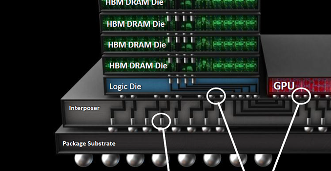
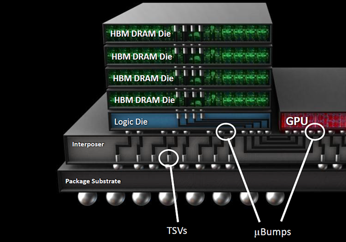
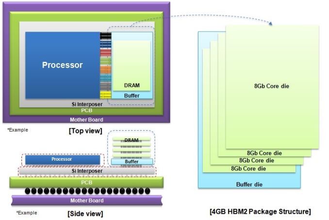
The original JESD235 standard defines the first-generation HBM (HBM1) memory chips with a 1024-bit interface and up to 1 Gb/s data-rate, which stack two, four or eight DRAM devices with two 128-bit channels per device on a base logic die. Each HBM stack (which is also called KGSD — known good stacked die) supports up to eight 128-bit channels because its physical interface is limited to 1024 bits. Every channel is essentially a 128-bit DDR interface with 2n prefetch architecture (256 bits per memory read and write access) that has its own DRAM banks (8 or 16 banks, depending on density), command and data interface, clock-rate, timings, etc. Each channel can work independently from other channels in the stack or even within one DRAM die. HBM stacks use passive silicon interposers to connect to host processors (e.g., GPUs). For more information about HBM check out our article called “AMD Dives Deep On High Bandwidth Memory — What Will HBM Bring AMD?”.
HBM gen 1 memory KGSDs produced by SK Hynix (the only company that makes them commercially) stack four 2 Gb memory dies and operate at 1 Gb/s data rate per pin. AMD uses these KGSDs with 1 GB capacity and 128 GB/s peak bandwidth per stack to build its Fiji GPU system-in-packages (SiPs) and the Radeon R9 Fury/R9 Nano video cards. The graphics adapters have 4 GB of VRAM onboard, not a lot for 2016. While AMD’s flagship video cards do not seem to have capacity issues right now, 4 GB of memory per graphics adapter is a limitation. AMD’s latest graphics cards sport 512 GB/s of memory bandwidth, a massive amount by today’s standards, but even that amount could be a constraint for future high-end GPUs.
HBM Gen 2: Good Thing Gets Better
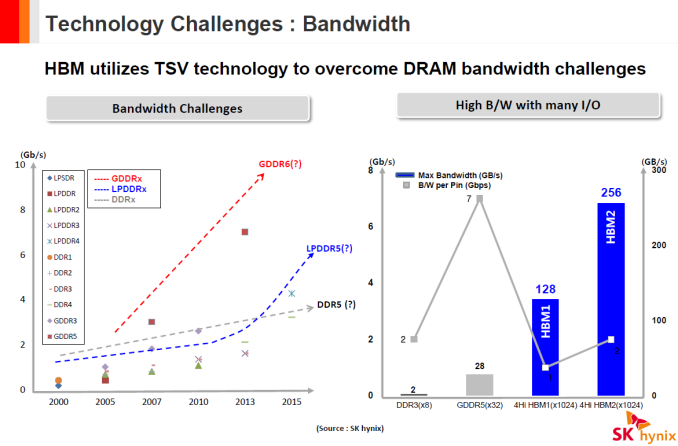
The second-generation HBM (HBM2) technology, which is outlined by the JESD235A standard, inherits physical 128-bit DDR interface with 2n prefetch architecture, internal organization, 1024-bit input/output, 1.2 V I/O and core voltages as well as all the crucial parts of the original tech. Just like the predecessor, HBM2 supports two, four or eight DRAM devices on a base logic die (2Hi, 4Hi, 8Hi stacks) per KGSD. HBM Gen 2 expands capacity of DRAM devices within a stack to 8 Gb and increases supported data-rates up to 1.6 Gb/s or even to 2 Gb/s per pin. In addition, the new technology brings an important improvement to maximize actual bandwidth.
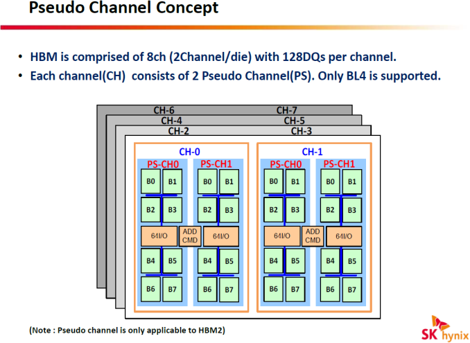
One of the key enhancements of HBM2 is its Pseudo Channel mode, which divides a channel into two individual sub-channels of 64 bit I/O each, providing 128-bit prefetch per memory read and write access for each one. Pseudo channels operate at the same clock-rate, they share row and column command bus as well as CK and CKE inputs. However, they have separated banks, they decode and execute commands individually. SK Hynix says that the Pseudo Channel mode optimizes memory accesses and lowers latency, which results in higher effective bandwidth.
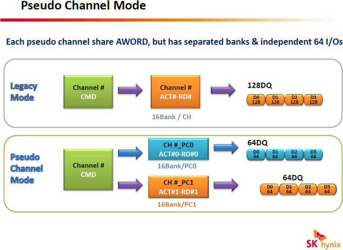
If, for some reason, an ASIC developer believes that Pseudo Channel mode is not optimal for their product, then HBM2 chips can also work in Legacy mode. While memory makers expect HBM2 to deliver higher effective bandwidth than predecessors, it depends on developers of memory controllers how efficient next-generation memory sub-systems will be. In any case, we will need to test actual hardware before we can confirm that HBM2 is better than HBM1 at the same clock-rate.
Additional improvements of HBM2 over the first-gen HBM includes lane remapping modes for hard and soft repair of lanes (HBM1 supports various DRAM cell test and repair techniques to improve yields of stacks, but not lane remapping), anti-overheating protection (KGSD can alert memory controllers of unsafe temperatures) and some other.
The second-generation HBM memory will be produced using newer manufacturing technologies than the first-gen HBM. For example, SK Hynix uses its 29nm process to make DRAM dies for its HBM1 stacks. For HBM2 memory, the company intends to use their 21nm process. Thanks to newer manufacturing technologies and higher effective bandwidth, HBM2 should have higher energy efficiency than HBM1 at its data-rates, but we do not have exact details at this point. In any case, HBM2 is likely to be more energy efficient than GDDR5 and GDDR5X, hence the odds are good that it will be the memory of choice for high-end graphics cards in the future.
Samsung Electronics this week said that it had begun mass production of HBM2 memory, but did not reveal too many details. Samsung’s HBM2 KGSD features 4 GB capacity, 2 Gb/s data rate per pin and is based on four 8 Gb DRAM dies. The memory chips will let device manufacturers build SiPs with up to 16 GB of memory. It is noteworthy that Samsung decided to use 8 Gb DRAM dies for its HBM2 stacks. Such decision looks quite logical since with 8 Gb DRAM ICs the company can relatively easily increase or decrease capacity of its KGSDs by altering the number of DRAM layers. The DRAM maker uses its 20nm process to produce its HBM2 DRAM KGSDs. Unfortunately, Samsung did not reveal actual power consumption of the new memory stacks.
| GPU Memory Math | |||||||
| AMD Radeon R9 290X | NVIDIA GeForce GTX 980 Ti | AMD Radeon R9 Fury X | Samsung’s 4-Stack HBM2 based on 8 Gb DRAMs | Theoretical GDDR5X 256-bit sub-system | |||
| Total Capacity | 4 GB | 6 GB | 4 GB | 16 GB | 8 GB | ||
| Bandwidth Per Pin | 5 Gb/s | 7 Gb/s | 1 Gb/s | 2 Gb/s | 10 Gb/s | ||
| Number of Chips/Stacks | 16 | 12 | 4 | 4 | 8 | ||
| Bandwidth Per Chip/Stack | 20 GB/s | 28 GB/s | 128 GB/s | 256 GB/s | 40 GB/s | ||
| Effective Bus Width | 512-bit | 384-bit | 4096-bit | 4096-bit | 256-bit | ||
| Total Bandwidth | 320 GB/s | 336 GB/s | 512 GB/s | 1 TB/s | 320 GB/s | ||
| Estimated DRAM Power Consumption |
30W | 31.5W | 14.6W | n/a | 20W | ||
Larger Package
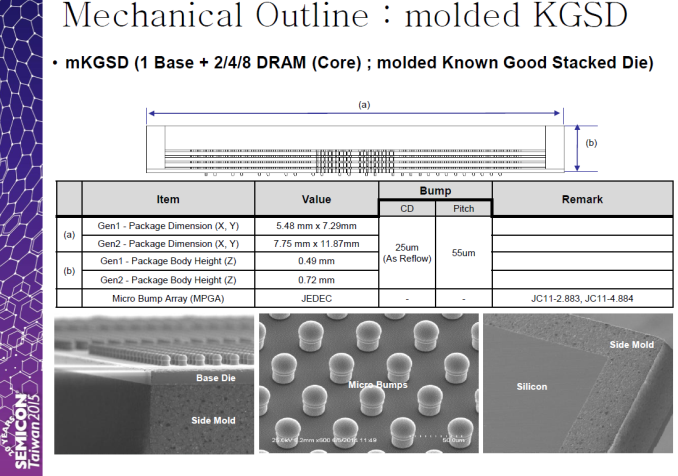
HBM2 memory stacks are not only faster and more capacious than HBM1 KGSDs, but they are also larger. SK Hynix’s HBM1 package has dimensions of 5.48 mm × 7.29 mm (39.94 mm2). The company’s HBM2 chip will have dimensions of 7.75 mm × 11.87 mm (91.99 mm2). Besides, HBM2 stacks will also be higher (0.695 mm/0.72 mm/0.745 mm vs. 0.49 mm) than HBM1 KGSDs, which may require developers of ASICs (e.g., GPUs) to install a heat-spreader on their SiPs to compensate for any differences in height between the memory stacks and GPU die, to protect the DRAM, and to guarantee sufficient cooling for high bandwidth memory.
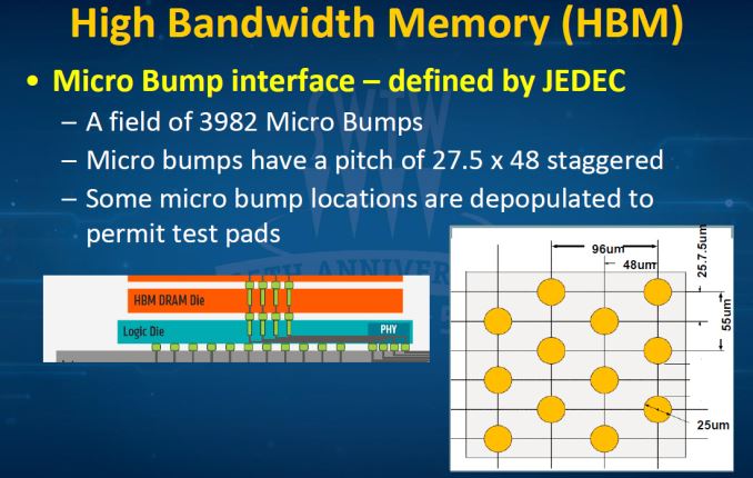
Larger footprint of the second-gen HBM2 means that the upcoming SiPs with multiple memory stacks will require larger silicon interposers, which means that they are going to be slightly more expensive than SiPs based on the first-gen HBM. Since geometric parameters of staggered microbump pattern of HBM1 and HBM2 are the same, complexity of passive silicon interposers will remain the same for both types of memory. A good news is that to enable 512 GB/s of bandwidth, only two HBM2 stacks are needed, which implies that from bandwidth per mm2 point of view the new memory tech continues to be very efficient.
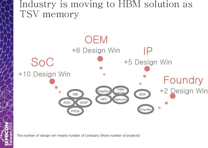
A slide by FormFactor and Teradyne from their presentation at Semiconductor Wafer Test Workshop 2015
Since SK Hynix’s HBM1 KGSDs are smaller than the company’s HBM2 stacks, they are going to have an advantage over the second-gen high-bandwidth memory for small form-factor SiPs. As a result, the South Korea-based DRAM maker may retain production of its HBM1 chips for some time.
New Use Cases and Industry Support
Thanks to higher capacity and data-rates, HBM2 memory stacks will be pretty flexible when it comes to configurations. For example, it will be possible to build a 2 GB KGSD with 256 GB/s of bandwidth that will use only two 8 Gb memory dies. Such memory stack could be used for graphics adapters designed for notebooks or ultra-small personal computers. Besides, it could be used as an external cache for a hybrid microprocessor with built-in graphics (in the same manner as Intel uses its eDRAM cache to boost performance of its integrated graphics processors). What remains to be seen is the cost of HBM2 stacks that deliver 256 GB/s bandwidth. If HBM2 and the necessary interposer remains as expensive as HBM1, it will likely continue to only be used for premium solutions.
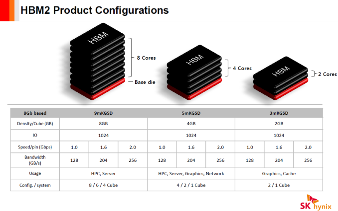
Thanks to a variety of KGSD configurations prepared by DRAM manufacturers, expect new types of devices to start using HBM2. Samsung and SK Hynix believe that in addition to graphics and HPC (high-performance computing) cards, various server, networking and other applications will utilize the new type of memory. As of September, 2015, more than 10 companies were developing system-on-chips (including ASICs, x86 processors, ASSPs and FPGAs) with HBM support, according to SK Hynix.
The first-generation HBM memory delivers great bandwidth and energy efficiency, but it is produced by only one maker of DRAM and is not widely supported by developers of various ASICs. By contrast, Samsung Electronics and SK Hynix, two companies that control well over 50% of the global DRAM output, will make HBM2. Micron Technology yet has to confirm its plans to build HBM2, but since this is an industry-standard type of memory, the door is open if the company wishes to produce it.
Overall, the industry support for the high bandwidth memory technology is growing. There are 10 companies working on SoCs with HBM support, leading DRAM makers are gearing up to produce HBM2. The potential of the second-gen HBM seems to be rather high, but the costs remain a major concern. Regardless, it will be extremely interesting to see next-generation graphics cards from AMD and NVIDIA featuring HBM2 DRAM and find out what they are capable of because of the new Polaris and Pascal architectures as well as the new type of memory.