

News


AMD To Spin-Off Back-End Testing & Assembly Operations Into Joint Venture For $371 Million

AMD To Spin-Off Back-End Testing & Assembly Operations Into Joint Venture For $371 Million

AMD’s Q3 2015 earnings release just hit the wire a bit ago, and while we’re still working on putting together that story we wanted to immediately jump into what is the biggest news to come out of today’s release. As part of their wave of news releases this afternoon, AMD is announcing that they will be spinning off their back-end manufacturing operations into a new joint venture with Nantong Fujitsu Microelectronics (NFME), with NFME essentially buying the bulk of these operations off of AMD.

Briefly then, in the world of semiconductor manufacturing the complete process of creating a chip is divided into two halves. There is the front-end manufacturing step where a complete wafer of chips is fabbed, and the back-end manufacturing step where those finished wafers are tested and cut up into individual chips for customer use. Dubbed ATMP – for assembly, test, mark, and pack – these back-end operations are in modern times split up from the fabbing step for cost reasons. Consequently capital-intensive and technologically advanced fabbing process will take place in facilities like TSMC Taiwan, GlobalFoundries Germany, and Intel US, while ATMP takes place at facilities in China, Malaysia, and Vietnam.

Up until their spin-off of GlobalFoundries in 2009, AMD had a complete chip manufacturing operation, including facilities for both the fabbing and ATMP operations. Even after the spin-off however, AMD held on to their ATMP operations. It is these operations that AMD is now spinning-off as well, as the company pursues an operations strategy more befitting of a fabless semiconductor designer.
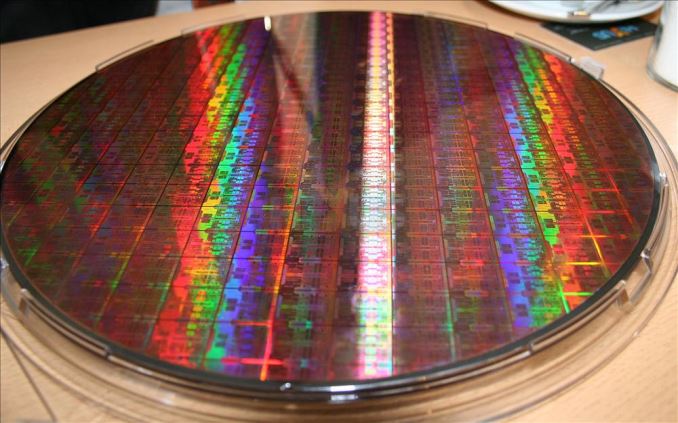

An AMD CPU Wafer (Image Courtesy Hexus.net)

For the deal with NFME, AMD will be spinning-off their ATMP operations into a new, unnamed joint venture in partnership with NFME. The joint venture will see AMD contribute their ATMP facilities in Penang, Malaysia and Suzhou, China, along with their roughly 1,700 person ATMP staff. Meanwhile, though not mentioned in the release, NFME will be contributing their own facilities and employees as well, with the complete joint venture set to have 5,800 employees spread over five facilities.

On the financial side of matters, NFME will immediately be buying an 85% stake of AMD’s ATMP operations, putting NFME in control of the overall joint venture while AMD serves as the minority partner with their remaining 15% share. In turn, NFME will be paying AMD approximately $371 million, and after taxes and other costs this will be a net gain of about $320 million for AMD.

Overall AMD is touting this as a beneficial change for the company, though they also don’t attempt to hide their current financial state in the announcement, stating that the joint venture and sale “further strengthens our balance sheet with significant asset monetization.” AMD on the whole has been struggling with a series of losses over what has now been a number of years, and it has taken a toll on their cash reserves. In the last few years the company has been slowly selling off non-essential or legacy assets in order to both contain ongoing costs and to raise much-needed cash for day-to-day operations. This, among other things, has included selling off and then leasing back their “Lone Star” campus in Austin, Texas.
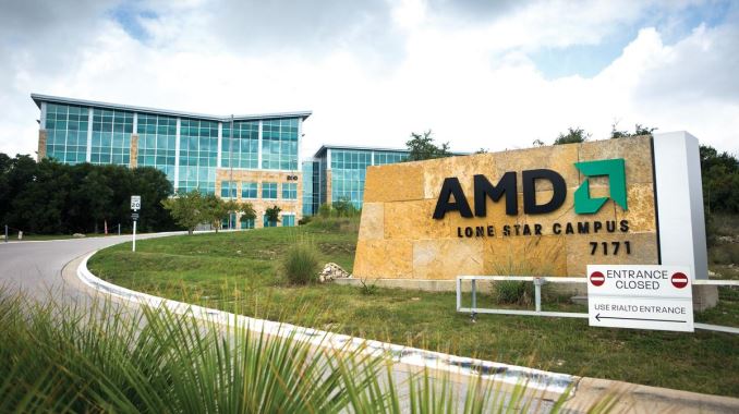

AMD’s Leased Lone Star Campus (Image Courtesy Austin Business Journal)

For AMD, the spin-off means they will be removing 1,700 employees from their payroll, which would put their adjusted headcount at around 7,500 to 8,000 employees after the deal closes. Furthermore as ATMP is capital-intensive, this allows AMD to further contain their spending on capital expenditures. AMD has until now held on to their ATMP operations, and at the time of the GlobalFoundries deal stated that they were keeping these operations as they were specifically tailored to AMD’s microprocessor business. However there’s no doubt that the have been an increasing drag on AMD as the company’s revenues and chip volume have continued to shrink. Ultimately as AMD was already fabless, it’s rare to see a fabless company with their own back-end operations anyhow, and AMD believes they can continue to meet their ATMP needs through this joint venture.

As for the joint venture itself, this gives NFME the ability to further expand into the market for semiconductor assembly and test services (SATS). With AMD’s lower product volumes no doubt making it harder to fully utilize their high-volume AMTP facilities, a joint venture with NFME can bring more work into those facilities by having them work for additional customers beyond AMD. Furthermore NVME also gains the R&D experience that comes with AMD’s AMTP operations, which for them is a competitive advantage against other 3rd party SATS providers.

Ultimately today’s announcement of a joint venture is at best mixed news for AMD. Containing costs is important for the company’s ongoing health and clearly the company no longer has the resources or demand to stay in any kind of manufacturing. On the other hand as the company continues to sell off assets in one form or another – and all the while continues to lose cash as happened again this quarter – it puts them in a perilous position of having to operate off of fewer and fewer assets. So hopefully this joint venture and accompanying sale helps the company focus on the chip and architectural development they need to do, and provide the funding over the next few years to accomplish it.

AMD To Spin-Off Back-End Testing & Assembly Operations Into Joint Venture For $371 Million

AMD To Spin-Off Back-End Testing & Assembly Operations Into Joint Venture For $371 Million

AMD’s Q3 2015 earnings release just hit the wire a bit ago, and while we’re still working on putting together that story we wanted to immediately jump into what is the biggest news to come out of today’s release. As part of their wave of news releases this afternoon, AMD is announcing that they will be spinning off their back-end manufacturing operations into a new joint venture with Nantong Fujitsu Microelectronics (NFME), with NFME essentially buying the bulk of these operations off of AMD.

Briefly then, in the world of semiconductor manufacturing the complete process of creating a chip is divided into two halves. There is the front-end manufacturing step where a complete wafer of chips is fabbed, and the back-end manufacturing step where those finished wafers are tested and cut up into individual chips for customer use. Dubbed ATMP – for assembly, test, mark, and pack – these back-end operations are in modern times split up from the fabbing step for cost reasons. Consequently capital-intensive and technologically advanced fabbing process will take place in facilities like TSMC Taiwan, GlobalFoundries Germany, and Intel US, while ATMP takes place at facilities in China, Malaysia, and Vietnam.

Up until their spin-off of GlobalFoundries in 2009, AMD had a complete chip manufacturing operation, including facilities for both the fabbing and ATMP operations. Even after the spin-off however, AMD held on to their ATMP operations. It is these operations that AMD is now spinning-off as well, as the company pursues an operations strategy more befitting of a fabless semiconductor designer.


An AMD CPU Wafer (Image Courtesy Hexus.net)

For the deal with NFME, AMD will be spinning-off their ATMP operations into a new, unnamed joint venture in partnership with NFME. The joint venture will see AMD contribute their ATMP facilities in Penang, Malaysia and Suzhou, China, along with their roughly 1,700 person ATMP staff. Meanwhile, though not mentioned in the release, NFME will be contributing their own facilities and employees as well, with the complete joint venture set to have 5,800 employees spread over five facilities.

On the financial side of matters, NFME will immediately be buying an 85% stake of AMD’s ATMP operations, putting NFME in control of the overall joint venture while AMD serves as the minority partner with their remaining 15% share. In turn, NFME will be paying AMD approximately $371 million, and after taxes and other costs this will be a net gain of about $320 million for AMD.

Overall AMD is touting this as a beneficial change for the company, though they also don’t attempt to hide their current financial state in the announcement, stating that the joint venture and sale “further strengthens our balance sheet with significant asset monetization.” AMD on the whole has been struggling with a series of losses over what has now been a number of years, and it has taken a toll on their cash reserves. In the last few years the company has been slowly selling off non-essential or legacy assets in order to both contain ongoing costs and to raise much-needed cash for day-to-day operations. This, among other things, has included selling off and then leasing back their “Lone Star” campus in Austin, Texas.


AMD’s Leased Lone Star Campus (Image Courtesy Austin Business Journal)

For AMD, the spin-off means they will be removing 1,700 employees from their payroll, which would put their adjusted headcount at around 7,500 to 8,000 employees after the deal closes. Furthermore as ATMP is capital-intensive, this allows AMD to further contain their spending on capital expenditures. AMD has until now held on to their ATMP operations, and at the time of the GlobalFoundries deal stated that they were keeping these operations as they were specifically tailored to AMD’s microprocessor business. However there’s no doubt that the have been an increasing drag on AMD as the company’s revenues and chip volume have continued to shrink. Ultimately as AMD was already fabless, it’s rare to see a fabless company with their own back-end operations anyhow, and AMD believes they can continue to meet their ATMP needs through this joint venture.

As for the joint venture itself, this gives NFME the ability to further expand into the market for semiconductor assembly and test services (SATS). With AMD’s lower product volumes no doubt making it harder to fully utilize their high-volume AMTP facilities, a joint venture with NFME can bring more work into those facilities by having them work for additional customers beyond AMD. Furthermore NVME also gains the R&D experience that comes with AMD’s AMTP operations, which for them is a competitive advantage against other 3rd party SATS providers.

Ultimately today’s announcement of a joint venture is at best mixed news for AMD. Containing costs is important for the company’s ongoing health and clearly the company no longer has the resources or demand to stay in any kind of manufacturing. On the other hand as the company continues to sell off assets in one form or another – and all the while continues to lose cash as happened again this quarter – it puts them in a perilous position of having to operate off of fewer and fewer assets. So hopefully this joint venture and accompanying sale helps the company focus on the chip and architectural development they need to do, and provide the funding over the next few years to accomplish it.
OCZ Announces First SATA Host Managed SSD: Saber 1000 HMS

OCZ Announces First SATA Host Managed SSD: Saber 1000 HMS

Today OCZ is introducing the first SATA drive featuring a technology that may be the next big thing for enterprise SSDs. Referred to by OCZ as “Host Managed SSD” technology (HMS) and known elsewhere in the industry by the buzzword “Storage Intelligence”, the general idea is to let the host computer know more about what’s going on inside the SSD and to have more influence over how the SSD controller goes about its business.

Standardization efforts have been underway for more than a year in the committees for SAS, SATA, and NVMe, but OCZ’s implementation is a pre-standard design that may not be compatible with what is eventually ratified. To provide some degree of forwards compatibility, OCZ is releasing an open-source abstraction library to provide what they hope will be a hardware-agnostic interface that can be used with future HMS devices.

OCZ’s HMS implementation provides a vendor-specific extension of the ATA command set. A mode switch is required to access HMS features; when HMS mode is off the drive behaves like a normal non-HMS SATA drive and all background processing like garbage collection are managed autonomously by the SSD. When the HMS features are enabled, the host computer can request that the drive override normal operating procedure and disable all background processes, or to perform them as a high-priority task. If background processing is left disabled for too long, the drive will re-enable the background processing when needed and suffer the immediate performance penalty of the emergency garbage collection.

The intention is to allow better aggregate performance from an array of drives. An example OCZ gives is of an array divided into three pools of drives. At any given time, two pools are actively receiving writes, while the drives in the third pool are focusing solely on the “background” housekeeping operations. The two pools that are in active use defer all the background processing and operate with peak performance and consistency. By cycling the drive pools through the two modes, the intention is that none of the active drives will ever reach the steady-state of having constant background processing to free up space for the incoming writes. This provides a big improvement to performance consistency, and can also provide a minor improvement to overall throughput of the array.

Obviously, the load balancing and coordination required by such a scheme is not part of any traditional RAID setup. OCZ expects early adopters of HMS technology to make use of it from application layer code. HMS does not require any new operating system drivers, and OCZ will be providing tools and reference code to facilitate using HMS. They plan to eventually expand this to a comprehensive SDK, but for now everybody is in the position of having to explore how to best make use of HMS for their specific use case. For some customers, that may mean load balancing several pools of SSDs attached to a single server, while others may find it easier to temporarily offline an entire server for housekeeping.

OCZ has also envisioned that future HMS products may expand the controls from managing background processing to also changing overprovisioning or power limits on the fly, but they have no specific timeline for those features.

The drive OCZ is introducing with HMS technology is a variant of their existing Saber 1000 enterprise SATA SSD. The Saber 1000 HMS differs only in the SSD controller firmware; otherwise it is still a low-cost drive using the Barefoot 3 controller and is intended primarily for read-oriented workloads. Pricing is the same with or without HMS capability, though the Saber 1000 HMS is only offered in the 480GB and 960GB capacities. The warranty in either case is limited to 5 years, but because the HMS controls can affect write amplification, the Saber HMS write endurance rating is based on the actual Program/Erase cycle count of the drive rather than the total amount of data written to the drive.

OCZ Saber 1000 HMS
Capacity 480GB 960GB
4kB Random Read IOPS 90k 91k
4kB Random Write IOPS 22k 16k
Random Read Latency 135µs 135µs
Random Write Latency 55µs 55µs
Sequential Read 550 MB/s 550 MB/s
Sequential Write 475 MB/s 445 MB.s
MSRP $370 $713

As a read-oriented drive with relatively little overprovisioning, the Saber 1000 has a lot to gain from HMS in terms of write performance and consistency, and it may allow the Saber 1000 HMS to compete in areas the Saber 1000 isn’t fast enough for.

In addition to control over the garbage collection process, the Saber 1000 HMS provides a similar set of controls for managing when the controller saves metadata from its RAM to the flash. This is the information the controller uses to keep track of where each piece of data is physically stored and which blocks are free to accept new writes. Every write to the disk adds to the metadata log, so the changes need to be periodically evicted from RAM to flash. This is one of the key data structures that the drive’s power loss protection needs to preserve, so the size of the in-RAM metadata log may also be limited by the drive’s capacitor budget.

To enable software to make effective use of these controls, the Saber 1000 HMS provides an unprecedented view in to the inner workings of the drive. Software can query the drive for the NAND page size, erase block size, number of blocks per bank and number of banks in the drive. The total program and erase counts are reported separately, and information about free blocks is reported as the total across the drive as well as the average, maximum, and minimum per bank. The drive also provides a status summary of whether garbage collection or metadata log dumping are active, and whether they are needed. OCZ’s reference guide provides recommendations for interpreting all of these indicators.

The Saber 1000 HMS will be available in early November for bulk purchases. The technical documentation and reference code should be available online today.