News


The Nexus 6 Review

When consumers think of Google’s Nexus devices, they think about the promise of receiving the latest updates for Android essentially as soon as they release. They also think about the value proposition that Nexus devices provide by giving good hardware at a price significantly lower than other smartphones. However, this was not always the case. The Nexus One, Nexus S, and Galaxy Nexus were all priced at the same level as other flagship smartphones. It was only with the launch of the Nexus 7 at $199 that we began to see a trend of inexpensive but still high quality devices coming from Google. That hasn’t changed at all in the past few weeks. The Nexus 5 and Nexus 7 are both still available, and they still provide a very high quality experience, arguably better than some other smartphones that are both newer and more expensive. But Google’s newest devices take aim directly at other flagship devices with both their specs and their prices. At $399 the Nexus 9 positions itself against Apple’s iPad Mini 3, while the Nexus 6 at $649 goes up against essentially every other flagship smartphone. Read on for our full review of Google’s Nexus 6.

Ingenic Launches Newton2: MIPS based IoT and Wearables Solution

Ingenic Launches Newton2: MIPS based IoT and Wearables Solution

The wearables and IoT market are moving very quickly, and only seven months after announcing their Newton platform, Ingenic is following up with Newton2. This pace reminds me of the glory days of consumer graphics cards, when NVIDIA and ATI were clawing for market share and would each produce two large launches per year. While the PC (and even smartphone) market has matured to a slower pace, the wearables and IoT market is currently quite frenetic. Dozens of companies worldwide are attempting to cash in on the explosive growth potential. Over time, we will see consolidation as contenders are crowned champions, but who those champions will be is anyone’s guess at the moment.

Ingenic is a relatively low profile company that could use an introduction. Ingenic is focused on semiconductors and devices and was founded in Beijing, China in 2005. Ingenic has licensed the MIPS architecture and designs their own CPU core and SoCs, and those designs are popular in low-end products such as digital picture frames, portable media players, and GPS devices. Ingenic had its IPO in 2011 and currently has a market cap of roughly $550 million.

Before getting to the details of Newton2, it’s important to understand positioning. Unlike other competitors, Ingenic positions the Newton (and Newton2) platform not as reference designs but instead as complete solutions. Ingenic would love to simply sell you the entire module as-is in high volume. However, Ingenic will build customized versions if you buy enough of them. This is similar to the Original Device Manufacturer (ODM) model, but in this case Newton is not an entire device but simply the electronics module. The purchaser still needs to place it into a full-fledged device like a smart watch or refrigerator. While Ingenic will sell you its custom designed SoCs as well, I am sure they would rather sell Newton as the margins for an integrated platform are guaranteed to be higher.

Now to the details. The Newton2 platform is a highly integrated module. These types of electronics are often referred to as a System on Module or SOM. Newton2 integrates the necessities of a wearable or IoT device, such as several built-in sensors and connectors for optional or obviously external components such as a display. Both Newton and Newton2 contain full featured application processors and can run Android.

Ingenic Newton2 SOM
Size 15mm x 30mm x 2.4mm
SoC Ingenic M200
Memory 512MB LPDDR2
Storage 4GB eMMC
WiFi Broadcom 43438 single-band 2.4GHz IEEE 802.11b/g/n
PMIC Ricoh RC5T619 power management IC
Bluetooth 4.1
Sensor IvenSense MPU-9250 gyroscope, accelerometer, magnetometer
Interfaces Display, Capacitive Touch, DMIC and AOHPL/R Audio, MIPI-CSI or I2C Camera, UART, I2C, GPIO, RF 2.4 GHz antenna, USB 2.0
Software Android 4.4

Power consumption for Newton is 4mW standby, 100mW average, and 260mW peak. Newton2 claims to cut standby consumption to 3mW.

The SoC on Newton2 is entirely new, the Ingenic M200. Notable inclusions in M200, beyond the bevy of traditional functionality, are the LCD and E-Ink display controllers, voice trigger processing offload, and the M200 SoC.

Ingenic M200 SoC
Package BGA270, 7.7mm x 8.9mm x 0.76mm, 0.4mm pitch
CPU XBurst1-HP core, 1.2 GHz
XBurst1-LP core, 300 MHz
GPU 2D/3D acceleration with OpenGL ES 2.0/1.1. OpenVG 1.1
VPU Video encoder up to 720p @ 30fps: H.264, VP8
Video decoder up to 720p @ 30fps: H.264, VP8, MPEG-1/2/4, VC-1, RV9
ISP HDR, video and image stabilization, crop and rescale, auto exposure + gain + white balance + focus control, edge sharpening, noise reduction, color correction, contrast enhancement, gamma correction
Memory DDR2, DDR3, LPDDR, LPDDR2 up to 667 Mbps
64-bit ECC NAND flash support Toggle 1.0 and ONFI2.0
Display LCD controller with OSD: TFT, SLCD and MIPI-DSI (2-lanes)
E-Ink controller
Camera MIPI-CSI2 (2-lanes), DVP
Audio Audio CODEC with 24-bit ADC/DAC, stereo line-in, MIC in, and headphone interface
Low power DMIC controller
AC97/I2S/SPDIF interface for external audio codec
One PCM interface, supports both master and slave modes
Voice trigger engine to wake system by programmable specific voice
ADC 3 channels 12-bit SAR
Interfaces USB 2.0 OTG x 1
MMC/SD/SDIO controller x 2
Full-duplex UART port x 5
Synchronous serial interface x 2
Two-wire SMB serial interface x 4
Software Android 4.4

Keep in mind that not every M200 interface is exposed on the Newton2. For example, accessing all five UARTs would require integrating the M200 into your own custom board.

The CPUs inside the M200 SOC set this SOM apart. The M200 integrates two custom designed Ingenic XBurst1 processors using the MIPS32 Release 2 ISA and include floating point and SIMD. Each processor is a full applications processor (AP) with an MMU and caches. However, you can consider the M200’s CPUs heterogeneous as one CPU is performance optimized and operates at up to 1.2 GHz while the other is optimized for power consumption and runs at up to 300 MHz. This is something we have seen before from NVIDIA with their Tegra devices as well as ARM’s big.LITTLE, but it’s different than other wearable and IoT efforts where low power duties are handled by a simple microcontroller (MCU). Using two APs likely simplifies software development somewhat, even if they are different, as they aren’t as enormously different as an AP and an MCU.

XBurst1 CPU
Pipeline 9-stage, single issue
Ingenic Estimated
Performance
2.0 DMIPS/MHz
ISA MIPS32 Release 2 (both Integer and Floating Point ISA)
XBurst SIMD
MMU 32 dual-entry full associative joint TLB
4 entry ITLB
4 entry DTLB
L1 Cache 32KB or 64KB I$ and D$
L2 Cache 256KB or 512KB
Debug EJTAG
Process 180nm, 90nm, 65nm, 40nm
Ingenic Estimated
Power Consumption
(1.0GHz, 0.09mW/MHz) @65nmLP
(1.2GHz, 0.07mW/MHz) @40nmLP, performance optimized
(500MHz, 0.05mW/MHz) @40nmLP, power optimized

Looking at the XBurst1 power consumption, these cores are significantly lower power than the Cortex-A5 which ARM specifies at 0.12 mW/MHz on the same 40nm LP process. Comparing these cores beyond their power consumption is outside the scope of this article, but it is worth pointing out because ARM is citing Cortex-A5 as their most power efficient wearable CPU.

The XBurst1 CPU core has been around since 2005, when Ingenic was founded. Ingenic revealed in 2013 it had purchased a MIPS64 license and was developing XBurst2 with design completion targeted at 2014. This will go hand in hand with Android 5.0 supporting MIPS64 ISA natively. Keeping with their roughly six month pace, it isn’t too farfetched to imagine a Newton3 platform sporting a MIPS64 XBurst2 with Android 5.0 launching in mid-2015.

Ingenic Launches Newton2: MIPS based IoT and Wearables Solution

Ingenic Launches Newton2: MIPS based IoT and Wearables Solution

The wearables and IoT market are moving very quickly, and only seven months after announcing their Newton platform, Ingenic is following up with Newton2. This pace reminds me of the glory days of consumer graphics cards, when NVIDIA and ATI were clawing for market share and would each produce two large launches per year. While the PC (and even smartphone) market has matured to a slower pace, the wearables and IoT market is currently quite frenetic. Dozens of companies worldwide are attempting to cash in on the explosive growth potential. Over time, we will see consolidation as contenders are crowned champions, but who those champions will be is anyone’s guess at the moment.

Ingenic is a relatively low profile company that could use an introduction. Ingenic is focused on semiconductors and devices and was founded in Beijing, China in 2005. Ingenic has licensed the MIPS architecture and designs their own CPU core and SoCs, and those designs are popular in low-end products such as digital picture frames, portable media players, and GPS devices. Ingenic had its IPO in 2011 and currently has a market cap of roughly $550 million.

Before getting to the details of Newton2, it’s important to understand positioning. Unlike other competitors, Ingenic positions the Newton (and Newton2) platform not as reference designs but instead as complete solutions. Ingenic would love to simply sell you the entire module as-is in high volume. However, Ingenic will build customized versions if you buy enough of them. This is similar to the Original Device Manufacturer (ODM) model, but in this case Newton is not an entire device but simply the electronics module. The purchaser still needs to place it into a full-fledged device like a smart watch or refrigerator. While Ingenic will sell you its custom designed SoCs as well, I am sure they would rather sell Newton as the margins for an integrated platform are guaranteed to be higher.

Now to the details. The Newton2 platform is a highly integrated module. These types of electronics are often referred to as a System on Module or SOM. Newton2 integrates the necessities of a wearable or IoT device, such as several built-in sensors and connectors for optional or obviously external components such as a display. Both Newton and Newton2 contain full featured application processors and can run Android.

Ingenic Newton2 SOM
Size 15mm x 30mm x 2.4mm
SoC Ingenic M200
Memory 512MB LPDDR2
Storage 4GB eMMC
WiFi Broadcom 43438 single-band 2.4GHz IEEE 802.11b/g/n
PMIC Ricoh RC5T619 power management IC
Bluetooth 4.1
Sensor IvenSense MPU-9250 gyroscope, accelerometer, magnetometer
Interfaces Display, Capacitive Touch, DMIC and AOHPL/R Audio, MIPI-CSI or I2C Camera, UART, I2C, GPIO, RF 2.4 GHz antenna, USB 2.0
Software Android 4.4

Power consumption for Newton is 4mW standby, 100mW average, and 260mW peak. Newton2 claims to cut standby consumption to 3mW.

The SoC on Newton2 is entirely new, the Ingenic M200. Notable inclusions in M200, beyond the bevy of traditional functionality, are the LCD and E-Ink display controllers, voice trigger processing offload, and the M200 SoC.

Ingenic M200 SoC
Package BGA270, 7.7mm x 8.9mm x 0.76mm, 0.4mm pitch
CPU XBurst1-HP core, 1.2 GHz
XBurst1-LP core, 300 MHz
GPU 2D/3D acceleration with OpenGL ES 2.0/1.1. OpenVG 1.1
VPU Video encoder up to 720p @ 30fps: H.264, VP8
Video decoder up to 720p @ 30fps: H.264, VP8, MPEG-1/2/4, VC-1, RV9
ISP HDR, video and image stabilization, crop and rescale, auto exposure + gain + white balance + focus control, edge sharpening, noise reduction, color correction, contrast enhancement, gamma correction
Memory DDR2, DDR3, LPDDR, LPDDR2 up to 667 Mbps
64-bit ECC NAND flash support Toggle 1.0 and ONFI2.0
Display LCD controller with OSD: TFT, SLCD and MIPI-DSI (2-lanes)
E-Ink controller
Camera MIPI-CSI2 (2-lanes), DVP
Audio Audio CODEC with 24-bit ADC/DAC, stereo line-in, MIC in, and headphone interface
Low power DMIC controller
AC97/I2S/SPDIF interface for external audio codec
One PCM interface, supports both master and slave modes
Voice trigger engine to wake system by programmable specific voice
ADC 3 channels 12-bit SAR
Interfaces USB 2.0 OTG x 1
MMC/SD/SDIO controller x 2
Full-duplex UART port x 5
Synchronous serial interface x 2
Two-wire SMB serial interface x 4
Software Android 4.4

Keep in mind that not every M200 interface is exposed on the Newton2. For example, accessing all five UARTs would require integrating the M200 into your own custom board.

The CPUs inside the M200 SOC set this SOM apart. The M200 integrates two custom designed Ingenic XBurst1 processors using the MIPS32 Release 2 ISA and include floating point and SIMD. Each processor is a full applications processor (AP) with an MMU and caches. However, you can consider the M200’s CPUs heterogeneous as one CPU is performance optimized and operates at up to 1.2 GHz while the other is optimized for power consumption and runs at up to 300 MHz. This is something we have seen before from NVIDIA with their Tegra devices as well as ARM’s big.LITTLE, but it’s different than other wearable and IoT efforts where low power duties are handled by a simple microcontroller (MCU). Using two APs likely simplifies software development somewhat, even if they are different, as they aren’t as enormously different as an AP and an MCU.

XBurst1 CPU
Pipeline 9-stage, single issue
Ingenic Estimated
Performance
2.0 DMIPS/MHz
ISA MIPS32 Release 2 (both Integer and Floating Point ISA)
XBurst SIMD
MMU 32 dual-entry full associative joint TLB
4 entry ITLB
4 entry DTLB
L1 Cache 32KB or 64KB I$ and D$
L2 Cache 256KB or 512KB
Debug EJTAG
Process 180nm, 90nm, 65nm, 40nm
Ingenic Estimated
Power Consumption
(1.0GHz, 0.09mW/MHz) @65nmLP
(1.2GHz, 0.07mW/MHz) @40nmLP, performance optimized
(500MHz, 0.05mW/MHz) @40nmLP, power optimized

Looking at the XBurst1 power consumption, these cores are significantly lower power than the Cortex-A5 which ARM specifies at 0.12 mW/MHz on the same 40nm LP process. Comparing these cores beyond their power consumption is outside the scope of this article, but it is worth pointing out because ARM is citing Cortex-A5 as their most power efficient wearable CPU.

The XBurst1 CPU core has been around since 2005, when Ingenic was founded. Ingenic revealed in 2013 it had purchased a MIPS64 license and was developing XBurst2 with design completion targeted at 2014. This will go hand in hand with Android 5.0 supporting MIPS64 ISA natively. Keeping with their roughly six month pace, it isn’t too farfetched to imagine a Newton3 platform sporting a MIPS64 XBurst2 with Android 5.0 launching in mid-2015.

Apple A8X’s GPU - GXA6850, Even Better Than I Thought

Apple A8X’s GPU – GXA6850, Even Better Than I Thought

Working on analyzing various Apple SoCs over the years has become a process of delightful frustration. Apple’s SoC development is consistently on the cutting edge, so it’s always great to see something new, but Apple has also developed a love for curveballs. Coupled with their infamous secrecy and general lack of willingness to talk about the fine technical details of some of their products, it’s easy to see how well Apple’s SoCs perform but it is a lot harder to figure out why this is.

Since publishing our initial iPad Air 2 review last week, a few new pieces of information have come in that have changed our perspective on Apple’s latest SoC. As it turns out I was wrong. Powered by what we’re going to call the GXA6850, the A8X’s GPU is even better than I thought.

Apple SoC Comparison
  A8X A8 A7 A6X
CPU 3x “Enhanced Cyclone” 2x “Enhanced Cyclone” 2x Cyclone 2x Swift
CPU Clockspeed 1.5GHz 1.4GHz 1.4GHz (iPad) 1.3GHz
GPU Apple/PVR GXA6850 PVR GX6450 PVR G6430 PVR SGX554 MP4
RAM 2GB 1GB 1GB 1GB
Memory Bus Width 128-bit 64-bit 64-bit 128-bit
Memory Bandwidth 25.6GB/sec 12.8GB/sec 12.8GB/sec 17.1GB/sec
L2 Cache 2MB 1MB 1MB 1MB
L3 Cache 4MB 4MB 4MB N/A
Transistor Count ~3B ~2B >1B N/A
Manufacturing Process TSMC(?) 20nm TSMC 20nm Samsung 28nm Samsung 32nm

Briefly, without a public die shot of A8X we have been left to wander through the dark a bit more than usual on its composition. A8X’s three “Enhanced Cyclone” CPU cores and 2MB of L2 cache were easy enough to discover, as the OS will cheerfully report those facts. However the GPU is more of an enigma since the OS does not report the GPU configuration and performance is a multi-variable equation that is reliant on both GPU clockspeed and GPU width (the number of clusters). Given Apple’s performance claims and our own benchmarks we believed we had sufficient information to identify this as Imagination’s PowerVR GX6650, the largest of Imagination’s GPU designs.

Since then, we have learned a few things that have led us to reevaluate our findings and discover that A8X’s GPU is even more powerful than GX6650. First and foremost, on Monday Imagination announced the PowerVR Series7 GPUs. Though not shipping for another year, we learned from Imagination’s announcement that Series7XT scales up to 16 clusters, twice the number of clusters as Series6XT. This immediately raises a red flag since Imagination never released an 8 cluster design – and indeed is why we believed it was GX6650 in the first place – warranting further investigation. This revelation meant that an 8 cluster design was possible, though by no means assured.


PowerVR Series7XT: Up 16 Clusters, Twice As Many As Series6XT

The second piece of information came from analyzing GFXBench 3.0 data to look for further evidence. While we don’t publish every single GFXBench subtest in our reviews, we still collect the data for Bench and for internal use. What we noticed is that the GFXBench fill rate test is showing more than double the performance of the A8 iPhone 6 Plus. Keeping in mind that performance here is a combination of width and clockspeed, fillrate alone does not prove an 8 cluster design or a 6 cluster design, only that the combination of width and clockspeeds leads to a certain level of performance. In other words, we couldn’t rule out a higher clocked GX6650.

GFXBench 3.0 Fill Rate Test (Offscreen)

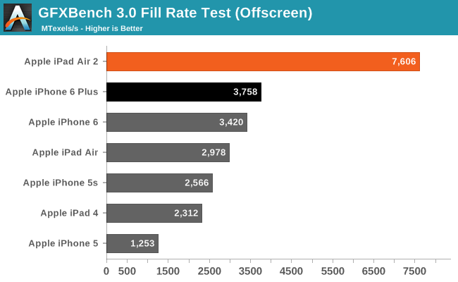
At the same time in the PC space the closest equivalent fillrate test, 3DMark Vantage’s pixel fill test, is known to be constrained by memory bandwidth as much as or more than it is GPU performance (this leading to the GTX 980’s incredible fillrate). However as we have theorized and since checked with other sources, GFXBench 3.0’s fillrate test is not bandwidth limited in the same way, at least not on Apple’s most recent SoCs. Quite possibly due to the 4MB of SRAM that is A7/A8/A8X’s L3 cache, this is a relatively “pure” test of pixel fillrate, meaning we can safely rule out any other effects.

With this in mind, normally Apple has a strong preference for wide-and-slow architectures in their GPUs. High clockspeeds require higher voltages, so going wide and staying with lower clockspeeds allows Apple to conserve power at the cost of some die space. This is the basic principle behind Cyclone and it has been the principle in Apple’s GPU choices as well. Given this, one could reasonably argue that A8X was using an 8 cluster design, but even with this data we were not entirely sure.

The final piece of the puzzle came in this afternoon when after some additional poking around we were provided with a die shot of A8X. Unfortunately at this point we have to stop and clarify that as part of our agreement with our source we are not allowed to publish this die shot. The die shot itself is legitimate, coming from a source capable of providing such die shots, however they didn’t wish to become involved in the analysis of the A8X and as a result we were only allowed to see it so long as we didn’t publish it.

Update: Chipworks has since published their A8X die shot, which we have reproduced below

To get right down to business then, the die shot confirms what we had begun suspecting: that A8X has an 8 cluster Series6XT configuration. All 8 GPU clusters are clearly visible, and perhaps unsurprisingly it looks a lot like the GPU layout of the GX6450. To put it in words, imagine A8’s GX6450 with another GX6450 placed right above it, and that would be the A8X’s 8 cluster GPU.


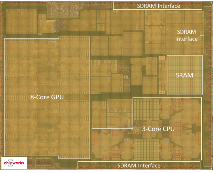
Chipworks A8X Die Shot

With 8 clearly visible GPU clusters, there is no question at this point that A8X is not using a GX6650, but rather something more. And this is perhaps where the most interesting point comes up, due to the fact that Imagination does not have an official 8 cluster Series6XT GPU design. While Apple licenses PowerVR GPU cores, not unlike their ARM IP license they are free to modify the Imagination designs to fit their needs, resulting in an unusual semi-custom aspect to their designs (and explaining what Apple has been doing with so many GPU engineers over the last couple of years). In this case it appears that Apple has taken the GX6450 design and created a new design from it, culminating in an 8 cluster Series6XT design. Officially this design has no public designation – while it’s based on an Imagination design it is not an official Imagination design, and of course Apple doesn’t reveal codenames – but for the sake of simplicity we are calling it the GXA6850.

Imagination/Apple PowerVR Series6XT GPU Comparison
  GXA6850 GX6650 GX6450 GX6250
Clusters 8 6 4 2
FP32 ALUs 256 192 128 64
FP32 FLOPs/Clock 512 384 256 128
FP16 FLOPs/Clock 1024 768 512 256
Pixels/Clock (ROPs) 16 12 8 4
Texels/Clock 16 12 8 4
OpenGL ES 3.1 3.1 3.1 3.1

Other than essentially doubling up on GX6450s, the GXA6850 appears to be unchanged from the design we saw in the A8. Apple did the necessary interconnect work to make an 8 cluster design functional and made their own power/design optimizations throughout the core, but there do not appear to be any further surprises in this GPU design. So what we have is an Apple variant on a Series6XT design, but something that is clearly a semi-custom Series6XT design and not a full in-house custom GPU design.


Unofficial GXA6850 Logical Diagram

Meanwhile the die shot places the die size of A8X at roughly 128mm2. This is in-line with our estimates – though certainly on the lower end – making A8X only a hair larger than the 123mm2 A6X. At roughly 3 billion transistors Apple has been able to increase their transistor count by nearly 50% while increasing the die size by only 40%, meaning Apple achieved better than linear scaling and A8X packs a higher average transistor density. On a size basis, A8X is a bit bigger than NVIDIA’s 118mm2 GK107 GPU or a bit smaller than Intel’s 2C+GT2 Haswell CPU, which measures in at 130mm2. Meanwhile on a transistor basis, as expected the 20nm A8X packs a far larger number of transistors than those 28nm/22nm products, with 3B transistors being larger than even Intel’s 4C+GT3 Haswell design (1.7B transistors) and right in between NVIDIA’s GK104 (3.5B) and GK106 (2.5B) GPUs.

Apple iPad SoC Evolution
  Die Size Transistors Process
A5 122mm2 <1B 45nm
A5X 165mm2 ? 45nm
A6X 123mm2 ? 32nm
A7 102mm2 >1B 28nm
A8X 128mm2 ~3B 20nm

Of this die space GXA6850 occupies 30% of A8X’s die, putting the GPU size at roughly 38mm2. This isn’t sufficient to infer the GPU transistor count, but in terms of absolute die size it’s still actually quite small thanks to the 20nm process. Roughly speaking an Intel Haswell GT2 GPU is 87mm2, but of course Apple has better density.

Moving on, the bigger question at this point remains why Apple went with an 8 cluster GPU over a 6 cluster GPU. From a performance standpoint this is greatly appreciated, but comparing iPad Air 2 to iPhone 6 Plus, the iPad Air 2 is nowhere near twice as many pixels as the iPhone 6 Plus. So the iPad Air 2 is “overweight” on GPU performance on a per-pixel basis versus its closest phone counterpart, offering roughly 30% better performance per pixel. Apple certainly has gaming ambitions with the iPad Air 2, and this will definitely help with that. But I believe there may also be a technical reason for such a large die.

The 128bit DDR3 memory bus used by the A8X requires pins, quite a lot in fact. Coupled with all of the other pins that need to come off of the SoC – NAND, display, audio, USB, WiFi, etc – and this is a lot of pins in a not very large area of space. At this point I am increasingly suspicious that Apple is pad limited, and that in order to fit a 128bit memory interface A8X needs to reach a minimum die size. With only a small organic substrate to help spread out pads, Apple has only as many pads as they can fit on the die, making a larger die a potential necessity. Ultimately if this were the case, Apple would have some nearly-free die space to spend on additional features if a 6 cluster A8X came in at under 128mm2, making the addition of 2 more clusters (~10mm2) a reasonable choice in this situation.

Finally, while we’re digging around in A8X’s internals, let’s quickly talk about the CPU block. There are no great surprises – nor did we expect to find any – but viewing the A8X die has confirmed that A8X is indeed an asymmetrical 3 CPU core design, and that there is no 4th (disabled) CPU core on the SoC. An odd number of CPU cores is unusual, though by no means unheard of. In this case Apple laid down a 3rd Enhanced Cyclone core, doubled the L2 cache, and left it at that.

Wrapping things up, it has become clear that with A8X Apple has once again thrown us a curveball. By drawing outside of the lines and building an eight cluster GPU configuration where none previously existed, the A8X and its GXA6850 GPU are more powerful than even we first suspected. Apple traditionally aims high with its SoCs, but this ended up being higher still.

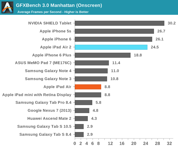
As far as performance is concerned this doesn’t change our initial conclusions – iPad Air 2 performs the same no matter how many GPU clusters we think are in it – but it helps to further explain iPad Air 2’s strong GPU performance. With 256 FP32 ALUs Apple has come very close to implementing a low-end desktop class GPU on a tablet SoC, and perhaps just as impressively can sustain that level of performance for hours. Though I don’t want to reduce this to a numbers war between A8X and NVIDIA’s TK1, it’s clear that these two SoCs stand apart from everything else in the tablet space.