News


Samsung Portable SSD T5 Review: 64-Layer V-NAND Debuts in Retail

​Samsung has been an active participant in the high-performance external SSD market with their Portable SSD series. The T1 was introduced in early 2015, while the T3 came out in early 2016. The T3 was the first retail product to utilize Samsung’s 48-layer TLC V-NAND. Today, Samsung is launching the Portable SSD T5. It is a retail pilot vehicle for their 64-layer TLC V-NAND as they ramp up its production. The Portable SSD T5 also moves up to a USB 3.1 Gen 2 Type-C interface, while retaining the same compact form factor and hardware encryption capabilities of the Portable SSD T3. Read on for our analysis of the product’s performance and value proposition.

Intel Officially Reveals Post-8th Generation Core Architecture Code Name: Ice Lake, Built on 10nm+

Intel Officially Reveals Post-8th Generation Core Architecture Code Name: Ice Lake, Built on 10nm+

In an unusual move for Intel, the chip giant has ever so slightly taken the wraps off of one of their future generation Core architectures. Basic information on the Ice Lake architecture has been published over on Intel’s codename decoder, officially confirming for the first time the existence of the architecture and that it will be made on Intel’s 10nm+ process.

The Ice Lake processor family is a successor to the 8th generation Intel® Core™ processor family. These processors utilize Intel’s industry-leading 10 nm+ process technology.

This is an unexpected development as the company has yet to formally detail (let alone launch) the first 10nm Core architecture –  Cannon Lake – and it’s rare these days for Intel to talk more than a generation ahead in CPU architectures. Equally as interesting is the fact that Intel is calling Ice Lake the successor to their upcoming 8th generation Coffee Lake processors, which codename bingo aside, throws some confusion on where the 14nm Coffee Lake and 10nm Cannon Lake will eventually stand.

As a refresher, the last few generations of Core have been Sandy Bridge, Ivy Bridge, Broadwell, Haswell, Skylake, with Kaby Lake being the latest and was recently released at the top of the year. Kaby Lake is Intel’s third Core product produced using a 14nm lithography process, specifically the second-generation ’14 PLUS’ (or 14+) version of Intel’s 14nm process.

Meanwhile when it comes to future products, back at CES Intel briefly showed a device based on post-Kaby Lake designs, called Cannon Lake and based on their 10nm process. Since then Intel has also confirmed that the 8th Generation of processors for desktops, called Coffee Lake, will be announced on August 21st (and we recently received promotional material to that effect). Ice Lake then, seems poised to follow both Coffee Lake and Cannon Lake, succeeding both architectures with a single architecture based on 10nm+.

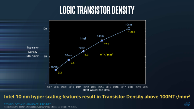
Working purely on lithographic nomenclature, Intel has three processes on 14nm: 14, 14+, and 14++. As shown to everyone at Intel’s Technology Manufacturing Day a couple of months ago, these will be followed by a trio of 10nm processes: 10nm, 10nm+ (10+), and 10++,

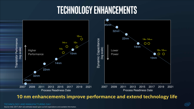
On the desktop, Core processors will go from 14 to 14+ to 14++, such that we move from Skylake to Kaby Lake to Coffee Lake. On the Laptop side, this goes from 14 to 14+ to 14++/10, such that we move from Skylake to Kaby Lake to Coffee Lake like the desktops, but also that at some time during the Coffee Lake generation, Cannon Lake will also be launched for laptops. The next node for both after this is 10+, which will be helmed by the Ice Lake architecture.

Intel’s Core Architecture Cadence
Microarchitecture Core Generation Process Node Release Year
Sandy Bridge 2nd 32nm 2011
Ivy Bridge 3rd 22nm 2012
Haswell 4th 22nm 2013
Broadwell 5th 14nm 2014
Skylake 6th 14nm 2015
Kaby Lake 7th 14nm+ 2016
Coffee Lake 8th 14nm++ 2017
Cannon Lake 8th? 10nm 2018?
Ice Lake 9th? 10nm+ 2018?

The way that the desktop and laptop markets will be diverging then converging is confusing a lot of people. Why is the laptop market splitting between 14++ and 10, and why is the desktop market not going to 10nm but straight to 10+? What lies beyond is a miasma of guess work, leaked slides, and guessing Intel’s strategy, but I believe the answer lies in Intel’s manufacturing technologies and the ability to move to newer lithographic nodes.

(We should interject here that the naming of a lithographic node has slowly lost its relevance between the features of the process and the actual transistor density and performance, such that TSMC’s improved 16FF+ is called 12FFN, but relies on similar transistor sizes with enhanced attributes. But 12 is a smaller number than 14, which is the marketing angle kicking in. By all accounts, Intel has typically been considered the more accurate foundry when it comes to numerical lithographic naming of the process, which others consider is to their detriment.)

Intel originally predicted that they would move to 10nm almost a year ago, at the end of 2016 and 2 years after the launch of their 14nm process. But the challenge in managing the technology required to advance to their version of 10nm has been fraught with difficulty. In all cases it can depend on external equipment, fine tuning a process, or getting acceptable yields – while one manufacturer might be satisfied with an 80% yield, another might consider that a failure. Being able to obtain high yields (ramp up) will also be a function of die size, and so the newest nodes are typically launched with smaller mobile parts in mind first, as the yields for smaller parts are better than larger parts at the same defect rate.

Simply put, the first generation of 10nm requires small processors to ensure high yields. Intel seems to be putting the smaller die sizes (i.e. anything under 15W for a laptop) into the 10nm Cannon Lake bucket, while the larger 35W+ chips will be on 14++ Coffee Lake, a tried and tested sub-node for larger CPUs. While the desktop sits on 14++ for a bit longer, it gives time for Intel to further develop their 10nm fabrication abilities, leading to their 10+ process for larger chips by working their other large chip segments (FPGA, MIC) first.

From a manufacturing standpoint, Intel has been using multiple patterning techniques in its 14nm processes, and the industry is looking to when the transition to EUV will take place. Anton has some great writeups of the state of EUV and how different companies are transitioning to smaller nodes – they are well worth a read.

The crux of the matter is that EUV would shorten time to market and arguably make the process easier (if only more expensive), and several fab companies are waiting for Intel to jump onto it first. With EUV not ready, Intel has had to invest into deeper multi-patterning techniques, which raise costs, decrease yields, and increase wafer process times considerably.

All of which leads to a miasma of increased delays, much to the potential chagrin of investors but also customers who had banked on the power improvements that a typical new lithography node brings. Intel is still keeping spirits high, by producing numbers that would suggest that their methodology is still in tune with Moore’s Law, even if the products seem to be further strung out. Some analysts concur with Intel’s statements, while others see it as hand-waving until 10/10+ hits the market. Intel would also point out that it is developing other technologies such as Embedded Multi-Die Interconnect Bridges (EMIB) to assist in equipping chip with high-speed fabric or glue-logic.

Given its position as a post-8th gen architecture, Ice Lake is likely to hit sometime in 2018, perhaps 2019, depending on Intel’s rate of progress with larger chips and the 10+ process. Intel’s other market segments, such as FPGAs (Altera), Xeon Phi (MIC) and custom foundry partners, are also in the mix to get into some 10nm action.

(Note that Intel’s next generation of Xeon Scalable Processors is called Cascade Lake, a 2018 refresh of the Skylake generation launched this year.)

The Toshiba XG5 (1TB) SSD Review

The Toshiba XG5 is their first SSD to ship with 64-layer 3D NAND and is their first mainstream SSD to use 3D NAND. The XG5 is a NVMe SSD with TLC NAND intended for OEMs. It aims to provide a balance of high performance, low power, and affordability. As our first hands-on testing of Toshiba’s 3D NAND, the XG5 previews the advancements 3D NAND will be bringing to Toshiba’s entire SSD lineup and SSDs from many other brands.

Toshiba Announces BG3 Low-Power NVMe SSD With BiCS3 3D NAND

Toshiba Announces BG3 Low-Power NVMe SSD With BiCS3 3D NAND

Toshiba’s transition to their 64-layer 3D NAND flash memory continues predictably with today’s launch of their third-generation BGA SSD, the BG3 series. First unveiled in 2015, Toshiba’s family of BGA SSDs serves as their entry-level client OEM NVMe offering, with a focus on low power use and compact packaging rather than high performance. A year ago, Toshiba’s BG series became their first client SSD to adopt their 3D NAND and it was one of only a handful of products to use their 48-layer BiCS2 3D NAND. This year, Toshiba finally has 3D NAND suitable for widespread adoption in their 64-layer BiCS3 3D NAND. The BG3 is their third SSD announced with the new 3D NAND, after the XG5 mainstream NVMe SSD for the OEM market and the TR200 retail SATA SSD. So far, all of Toshiba’s 64-layer 3D NAND SSDs are using the 3-bit-per-cell TLC variant.

Aside from the update to the new generation of 3D NAND, little has changed with the BG series over the previous generation. The BG3 still uses the standard M.2 16x20mm BGA package with a PCIe 3 x2 link. As with the last generation, the BG3 is a DRAM-less SSD that supports the NVMe 1.2 Host Memory Buffer feature to mitigate the performance impact of not including DRAM on the SSD itself. The BG3 uses only about 38MB of the host system’s RAM to cache mapping information about which logical block addresses are stored in which flash memory pages. That 38MB cache is sufficient to provide a substantial performance boost for workloads with a working set in the 2GB to 16GB range, with Toshiba citing improvements of 80% to 150% for random accesses at high queue depths.

The BG3 will be available in the same three capacities from 128GB to 512GB, but the packaging has been slimmed slightly: the smaller two models are now 1.3mm thick instead of 1.4mm, and the 512GB model is now 1.5mm instead of 1.65mm. The BG3 will also be available mounted on a removable single-sided M.2 2230 card. The BG3 is rated for up to 1520 MB/s for sequential reads and 840MB/s for sequential writes, with a maximum power draw of 3.2W and a typical active power of 2.7W. As with all of their OEM SSDs, Toshiba is not disclosing exact pricing, but they say it is comparable to SATA drives. The BG3 is currently sampling to OEMs and will be on display at Flash Memory Summit next week.

Toshiba plans to continue transitioning to 64-layer 3D NAND in every segment of the SSD market. The OEM counterpart to the TR200 SATA SSD will be the Toshiba SG6, which will complete their client OEM lineup. We expect retail NVMe products to be announced later this year.

AMD Ryzen Threadripper 1950X and 1920X: We’re Allowed To Show Pictures Now

AMD Ryzen Threadripper 1950X and 1920X: We’re Allowed To Show Pictures Now

One of the interesting things to come out of this Threadripper launch is the stack of embargos. Last week AMD revealed the launch date and pricing, which will incidentally also be the date for our review of both chips. AMD also inserted a small embargo in the middle for today, allowing media outlets to do unboxings.

We’re Allowed To Show Pictures Now

Rather than discuss each element of what AMD shipped the ~250 reviewers who have review kits, this article is going to be mainly a picture story with annotations. Starting with a pelican case that AMD shipped the CPUs in.


Mug for Scale

Inside the massive padded box were two CPUs in special cases, along with a paperweight.

Yes, that’s an actual CPU in the paperweight, printed with AnandTech’s logo. We got CPU 30 out of 250.

Who has #1 ?

Each of the CPUs was in this overly padded secondary box.

 
Vital Codes

The instructions were far from clear. I tried to record this on video. Some swearing was involved – you definitely need two hands for this.

The CPU is housed in its own secondary support system. Twist, unlock, pull, grip, fail, try again, use force, swear, then eventually get the latch off.

The CPU comes in this orange holder. The orange holder goes into the motherboard as well, so there’s no need to take the CPU out.

The box also contains a bracket for Asetek liquid coolers to fit, and a Torx Screwdriver. There are some stickers as well.

Putting it in the socket is fairly easy – three Torx screws and the mechanism pops open. Slide into the tray, close the screws. I had more issues with the CPU cooler mechanism than the CPU tray.

This last picture shows how thermal paste spreads across the CPU after a couple of days of testing with a tight liquid cooler. We can’t say much about temperatures at this point because of the embargo.

Paperweight. No idea if the CPU inside actually works.

Along with the CPUs, AMD supplied almost everything needed for the system: an ASUS X399 Zenith Extreme motherboard, 32GB of G.Skill Trident RGB DDR4-3200 C14 memory, a 512GB Samsung 960 Pro M.2 drive, a Thermaltake Toughpower Grand 1200W, and a Thermaltake Floe Riing 360 Premium liquid cooler (a 3×120 side radiator). The only thing missing was a Vega GPU (ed: you don’t get everything).

What Does This Mean

I’ve never had a review sample come with quite so much kit in such extravagant packaging. Back with Ryzen they supplied a hardwood box with all the kit, and this one goes another stage up. AMD knows they can cause a stir on the social channels by being big and bright rather than staying understated, and to a certain extent, it works (as long as the company can afford it). It’s a corner of the product release cycle that AMD has honed in on, or one that its competitors have missed, although it is hard to gauge the return on investment and requires a marketing head to approve it nonetheless.

AMD Ryzen SKUs
  Cores/
Threads
Base/
Turbo
XFR L3 DRAM
1DPC
PCIe TDP Cost Cooler
TR 1950X 16/32 3.4/4.0 ? 32 MB 4×2666 60 180W $999
TR 1920X 12/24 3.5/4.0 ? 32 MB 4×2666 60 180W $799
TR 1900X 8/16 3.8/4.0 +200 ? 4-Ch 60 ? $549
Ryzen 7 1800X 8/16 3.6/4.0 +100 16 MB 2×2666 16 95 W $499
Ryzen 7 1700X 8/16 3.4/3.8 +100 16 MB 2×2666 16 95 W $399
Ryzen 7 1700 8/16 3.0/3.7 +50 16 MB 2×2666 16 65 W $329 Spire
Ryzen 5 1600X 6/12 3.6/4.0 +100 16 MB 2×2666 16 95 W $249
Ryzen 5 1600 6/12 3.2/3.6 +100 16 MB 2×2666 16 65 W $219 Spire
Ryzen 5 1500X 4/8 3.5/3.7 +200 16 MB 2×2666 16 65 W $189 Spire
Ryzen 5 1400 4/8 3.2/3.4 +50 8 MB 2×2666 16 65 W $169 Stealth
Ryzen 3 1300X 4/4 3.5/3.7 +200 8 MB 2×2666 16 65 W $129 Stealth
Ryzen 3 1200 4/4 3.1/3.4 +50 8 MB 2×2666 16 65 W $109 Stealth

What now? Time to get back to testing. Review next week. 

The Change in NDA Philosophy: A Personal Commentary

This new ‘unboxing’ sort of embargo has been borne from a rapid change in how media approaches launches and NDAs.

In the past, from 2014 and before, when there was a product NDA in place it was expected that no media would even acknowledge that they had the product, let alone disclose the date of launch. In the advent of a more social media focused – and younger – technology press, skirting those NDA lines with product images has now become almost a standard: if you have the product, flaunt it, and generate hype for the review/video. Even when there is an NDA in place specifically barring certain types of content, such as unboxings, it seems that posting screenshots or gifs of the upcoming unboxing content being edited before the NDA is becoming the norm.

The reasoning stems from the fact that NDAs typically restrict product reviews and only mention performance and data analysis to be revealed at a certain date, and the argument is that the NDAs often say nothing about showcasing the product before the launch (or even if the NDA is itself under NDA). Depending on the company, this has had a mixed response: typically an incumbent market leader will come down hard if NDA rules are pushed, although PR teams and underdogs like to push the hype train as many times around the track as possible if the product is good.

AnandTech in this respect is fairly old-school: we’d rather spend more time testing the product to give more data for our analysis and reviews, making sure our readers have the sufficient knowledge at hand to invest in a product. Unboxings on AT are few and far between because there usually isn’t that much to show for our typical user base that know technology – it only really makes sense to us when something is unusual (like Threadripper), or to show to new users that may become enthusiasts. Ultimately, it’s that latter group that has spurned the tech media to invest in social media for this sort of content, especially around high-performance components or hardware where it actually makes sense, like monitors. Unboxing products like a CPU would usually take several seconds: CPU, manual, cooler, sticker, done.

Related Reading