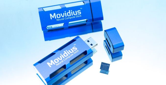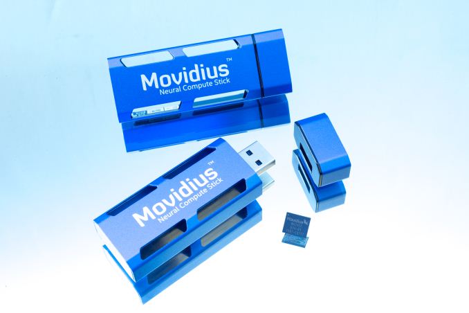
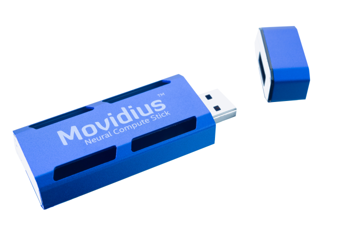
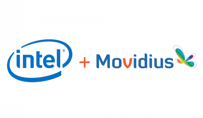
Today Intel subsidiary Movidius is launching their Neural Compute Stick (NCS), a version of which was showcased earlier this year at CES 2017. The Movidius NCS adds to Intel’s deep learning and AI development portfolio, building off of Movidius’ April 2016 launch of the Fathom NCS and Intel’s later acquisition of Movidius itself in September 2016. As Intel states, the Movidius NCS is “the world’s first self-contained AI accelerator in a USB format,” and is designed to allow host devices to process deep neural networks natively – or in other words, at the edge. In turn, this provides developers and researchers with a low power and low cost method to develop and optimize various offline AI applications.
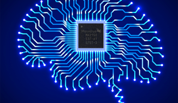
Movidius’s NCS is powered by their Myriad 2 vision processing unit (VPU), and, according to the company, can reach over 100 GFLOPs of performance within an nominal 1W of power consumption. Under the hood, the Movidius NCS works by translating a standard, trained Caffe-based convolutional neural network (CNN) into an embedded neural network that then runs on the VPU. In production workloads, the NCS can be used as a discrete accelerator for speeding up or offloading neural network tasks. Otherwise for development workloads, the company offers several developer-centric features, including layer-by-layer neural networks metrics to allow developers to analyze and optimize performance and power, and validation scripts to allow developers to compare the output of the NCS against the original PC model in order to ensure the accuracy of the NCS’s model.
The 2017 Movidius NCS vs. 2016 Fathom NCS
According to Gary Brown, VP of Marketing at Movidius, this ‘Acceleration mode’ is one of several features that differentiate the Movidius NCS from the Fathom NCS. The Movidius NCS also comes with a new “Multi-Stick mode” that allows multiple sticks in one host to work in conjunction in offloading work from the CPU. For multiple stick configurations, Movidius claims that they have confirmed linear performance increases up to 4 sticks in lab tests, and are currently validating 6 and 8 stick configurations. Importantly, the company believes that there is no theoretical maximum, and they expect that they can achieve similar linear behavior for more devices. Though ultimately scalability will depend at least somewhat with the neural network itself, and developers trying to use the feature will want to play around with it to determine how well they can reasonably scale.
Meanwhile, the on-chip memory has increased from 1 GB on the Fathom NCS to 4 GB LPDDR3 on the Movidius NCS, in order to facilitate larger and denser neural networks. And to cap it all off, Movidius has been able to reduce the MSRP to $79 – citing Intel’s “manufacturing and design expertise” – lowering the cost of entry even more.
Like other players in the edge inference market, Movidius is looking to promote and capitalize on the need for low-power but capable inference processors for stand-alone devices. That means targeting use cases where the latency of going to a server would be too great, a high-performance CPU too power hungry, or where privacy is a greater concern. In which case, the NCS and the underlying Myriad 2 VPU are Intel’s primary products for device manufacturers and software developers.
| Movidius Neural Compute Stick Products |
| |
Movidius Neural Compute Stick |
Fathom Neural Compute Stick |
| Interface |
USB 3.0 Type A |
USB 3 |
| On-chip Memory |
4Gb LPDDR3 |
1Gb/512Mb LPDDR3 |
| Deep Learning Framework Support |
Caffe |
Caffe
TensorFlow |
| Native Precision Support |
FP16 |
FP16, 8bit |
| Features |
Acceleration mode
Multi-Stick mode |
N/A |
| Nominal Power Envelope |
1W |
1W |
| SoC |
Myriad 2 VPU |
Myriad 2 VPU (MA2450) |
| Launch Date |
7/20/2017 |
4/28/2016 |
| MSRP |
$79 |
$99 |
As for the older Fathom NCS, the company notes that the Fathom NCS was only ever released in a private beta (which was free of charge). So the Movidius NCS is the de facto production version. For customers who did grab a Fathom NCS, Movidius says that Fathom developers will be able to retain their current hardware and software builds, but the company will be encouraging developers to switch over to the production-ready Movidius NCS.
Stepping back, it’s clear that the Movidius NCS offers stronger and more versatile features beyond the functions described in the original Fathom announcement. As it stands, the Movidius NCS offers native FP16 precision, with over 10 inferences per second at FP16 precision on GoogleNet in single-inference mode, putting it in the same range as the 15 nominal inferences per second of the Fathom. While the Fathom NCS was backwards compatible with USB 1.1 and USB 2, it was noted that the decreased bandwidth reduced performance; presumably, this applies for the Movidius NCS as well.

SoC-wise, while the older Fathom NCS had a Myriad 2 MA2450 variant, a specific Myriad 2 model was not described for the Movidius NCS. A pre-acquisition 2016 VPU product brief outlines 4 Myriad 2 family SoCs to be built on a 28nm HPC process, with the MA2450 supporting 4Gb LPDDR3 while the MA2455 supports 4Gb LPDDR3 and secure boot. Intel’s own Myriad 2 VPU Fact Sheet confirms the 28nm HPC process, implying that the VPU remains fabbed with TSMC. Given that the 2014 Myriad 2 platform specified a TSMC 28nm HPM process, as well as a smaller 5mm x 5mm package configuration, it’s possible that a different, more refined 28nm VPU powers the Movidius NCS. In any case, it was mentioned that the 1W power envelope applies to the Myriad 2 VPU, and that in certain complex cases, the NCS may operate within a 2.5W power envelope.
Ecosystem Transition: From Google’s Project Tango to Movidius, an Intel Company
Close followers of Movidius and the Myriad SoC family may recall Movidius’ previous close ties with Google, having announced a partnership with Myriad 1 in 2014, culminating in the Myriad 1’s appearance in Project Tango. Further agreements in January 2016 saw Google sourcing Myriad processors and Movidius’ entire software development environment in return for Google contributions to Movidius’ neural network technology roadmap. In the same vein, the original Fathom NCS also supported Google’s TensorFlow, in contrast to the Movidius NCS, which is only launching with Caffe support.
As an Intel subsidiary, Movidius has unsurprisingly shifted into Intel’s greater deep learning and AI ecosystem. On that matter, Intel’s acquisition announcement explicitly linked Movidius with Intel RealSense (which also found its way into Project Tango) and computer vision endeavors; though explicit Movidius integration with RealSense is yet to be seen – or if in the works, made public. In the official Movidius NCS news brief, Intel does describe Movidius fitting into Intel’s portfolio as an inference device, while training and optimizing neural networks falls to the Nervana cloud and Intel’s new Xeon Scalable processors respectively. To be clear, this doesn’t preclude Movidius NCS compatibility with other devices, and to that effect Mr. Brown commented: “If the network has been described in Caffe with the supported layer types, then we expect compatibility, but we also want to make clear that NCS is agnostic to how and where the network was trained.”
On a more concrete note, Movidius has a working demonstration of a Xeon/Nervana/Caffe/NCS workflow, where an end-to-end workflow of a Xeon-based training scheme generates a Caffe network optimized by Nervana’s Intel Caffe format, which is then deployed via NCS. Movidius plans to debut this demo at Computer Vision and Pattern Recognition (CVPR) conference in Honolulu, Hawaii later this week. In general, Movidius and Intel promise to have plenty to talk about in the future, where Mr. Brown comments: “We will have more to share about technical integrations later on, but we are actively pursuing the best end-to-end experience for training through to deployment of deep neural networks.”
Upcoming News and NCS Demos at CVPR

Alongside the Xeon/Caffe/Nervana/NCS workflow demo, Movidius has a slew of other things to showcase at CVPR 2017. Interestingly, Intel has described their presentations and demos as two separate Movidius and RealSense affairs, implying that the aforementioned Movidius/RealSense unification is still in the works.
For Movidius, Intel describes three demonstrations: “SDK Tools in Action,” “Multi-Stick Neural Network Scaling,” and “Multi-Stage Multi-Task Convolutional Neural Network (MTCNN).” The first revolves around the Movidius Neural Compute SDK and the platform API. The multi-stick demo showcases 4 Movidius NCS’ in accelerating object recognition. Finally, the third demo showcases Movidius NCS support for MTCNN, “a complex multi-stage neural network for facial recognition.” Meanwhile, Intel is introducing the RealSense D400 series, a depth-sensing camera family
The multi-stick demo is presumably what the company mentioned as a multi-stick demo that has been validated on three different host platforms: desktop CPU, laptop CPU, and a low-end SoC. The company also has a separate acceleration demo, where the Movidius NCS accelerates a Euclid developer module and offloads the CPUs, “freeing up the CPU for other tasks such as route planning or running application-level tasks.” The result is around double the framerate and a two-thirds power reduction.
All-in-all, Intel sees and outright states that they consider the Movidius NCS to be a means towards democratizing deep learning application development. As recent as this week, we’ve seen a similar approach as Intel’s recent 15.46 integrated graphics driver brought support for CV and AI workload acceleration on Intel integrated GPUs, tying in with Intel’s open source Compute Library for Deep Neural Networks (clDNN) and associated Computer Vision SDK and Deep Learning Deployment Toolkits. On a wider scale, Intel has already publicly positioned itself for deep learning in edge devices by way of their ubiquitous iGPUs, and Intel’s ambitions are highlighted by its recent history of machine learning and autonomous automotive oriented acquisitions: MobilEye, Movidius, Nervana, Yogitech, and Saffron.
As Intel pushes forward with machine learning development by way of edge devices, it will be very interesting to see how their burgeoning ecosystem coalesces. Like the original Fathom, the Movidius NCS is aimed at lowering the barriers to entry, and as the Fathom launch video supposes, a future where drones, surveillance cameras, robots, and any device can be made smart by “adding a visual cortex” that is the NCS.
With that said, however, technology is only half the challenge for Intel. Neural network inference at the edge is a popular subject for a number of tech companies, all of whom are jockeying for the lead position in what they consider a rapidly growing market. So while Intel has a strong hand with their technology, success here will mean that they need to be able to break into this new market in a convincing way, which is something they’ve struggled with in past SoC/mobile efforts. The fact that they already have a product stack via acquisitions may very well be the key factor here, since being late to the market has frequently been Intel’s Achilles’ heel in the past.
Wrapping things up, the Movidius NCS is now available for purchase for a MSRP of $79 through select distributors, as well as at CVPR.