SK Hynix Launches 72-Layer 256 Gb 3D TLC NAND with Increased Performance

SK Hynix has formally introduced its fourth-generation 3D NAND memory chips with 72 layers. Initially, the 3D TLC flash chips will be offered in 256 Gb configurations, but by the end of the year the manufacturer plans to introduce 72-layer 3D TLC NAND devices with 512 Gb capacities. All of SK Hynix’s fourth-gen 3D NAND chips will feature a larger block size, a lower programming time and a faster interface, which is expected to result in higher performance levels compared to the company’s third-gen ICs.
As reported previously, 72-layer 3D NAND is a very important product lineup for SK Hynix because the company plans to offer such memory for a wide range of applications, and because such memory allows it to use its production facilities more efficiently (at least, according to the manufacturer). The company has been experimenting with 3D NAND for quite a while and launched its first commercial 36-layer 128 Gb 3D MLC NAND (which it calls 3D-V2) chips in 2015. The 3D-V2 ICs were primarily used for removable storage devices, but the 256 Gb 48-layer 3D TLC NAND (3D-V3) ICs that hit mass production in late 2016 are used for removables, embedded storage and will be used for SSDs in the coming months.
The initial 72-layer 3D TLC NAND (3D-V4) chips do not increase capacity versus their direct predecessors, but decrease their die size by approximately 30%, allowing SK Hynix to fit more of such chips on a single wafer. Unfortunately it is hard to estimate how the 50% increase of the number of layers affects the length of SK Hynix’s manufacturing cycle and costs, as SK Hynix naturally does not make any additional disclosures. Moreover, the company does not reveal whether it uses string stacking technique and stacks two 36-layer wafers together, or uses etching and produces 72 layers “natively.”
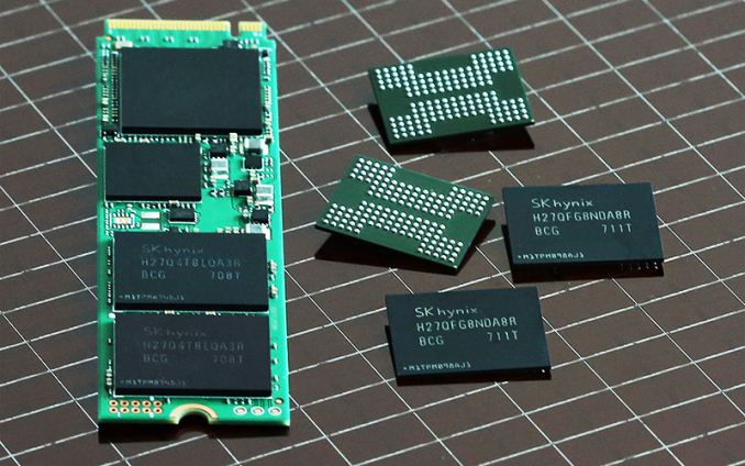
In addition to being smaller, the 72-layer 256 Gb 3D TLC NAND flash memory ICs also feature higher performance due to a 20% higher Toggle 2.0 interface data rate, a 50% larger block size compared to 48-layer 3D TLC chips (13.5 MB vs 9 MB) as well as a lower page programming time. SK Hynix does not disclose exact numbers for the interface and the tPROG, but it is logical to suspect that the new chips support 667 MT/s and, perhaps, 800 MT/s interface speed, just like some of the competing ICs. In any case, with increased block size and a lower tPROG (which SK Hynix calls 2x faster “internal operation speed”), any increase of the external interface speed from 533 MT/s of mainstream NAND today is more than welcome.
SK Hynix said it would start mass production of its 72-layer 256 Gb 3D TLC NAND (3D-V4) ICs in the second quarter of the year and such flash memory chips would be used for various storage devices (including those for mobile applications (e.g., smartphones)) in Q3 2017. The company’s product catalogue for Q1 2017 already lists 256 Gb 3D-V4 chips as well as multi-chip packages with 512 Gb – 4096 Gb (64 GB – 512 GB) capacities due to be available in Q2 2017 (such MCPs are used for mobiles). SSDs based on the new chips will be available after SK Hynix itself and its partners validate them, so, expect drives featuring the 48-layer 3D TLC NAND from the company to arrive first.
From SK Hynix’s Q1 2017 product catalogue we also know that later this year SK Hynix also plans to roll out 72-layer 512 Gb 3D TLC NAND chips (64 GB), which are expected to be available in Q4. It is crucially important for SK Hynix to increase the interface speed of its upcoming 3D-V4 ICs to 800 MT/s to reduce the performance penalty that comes from consolidating more flash onto fewer independent chips (and to stay competitive with Samsung’s 64-layer 512 Gb components). The upcoming ICs will enable the company as well as its partners to build higher-capacity storage solutions. For example, the SK Hynix’s catalogue lists a 8096 Gb (1 TB) MCPs based on the 512 Gb devices.
Related Reading:
- SK Hynix Lays Out Plans for 2017: 10nm-Class DRAM, 72-Layer 3D NAND
- SK Hynix to Build a New NAND Fab, Upgrade Existing DRAM Fab
- Toshiba Samples 64-Layer 512 Gb BiCS 3D NAND, Announces 1 TB BGA SSD
- Micron 2017 Roadmap Detailed: 64-layer 3D NAND, GDDR6 Getting Closer, & CEO Retiring
- Samsung at Flash Memory Summit: 64-layer V-NAND, Bigger SSDs, Z-SSD