

Estimating Intel-Micron 32-layer 3D NAND Die Size
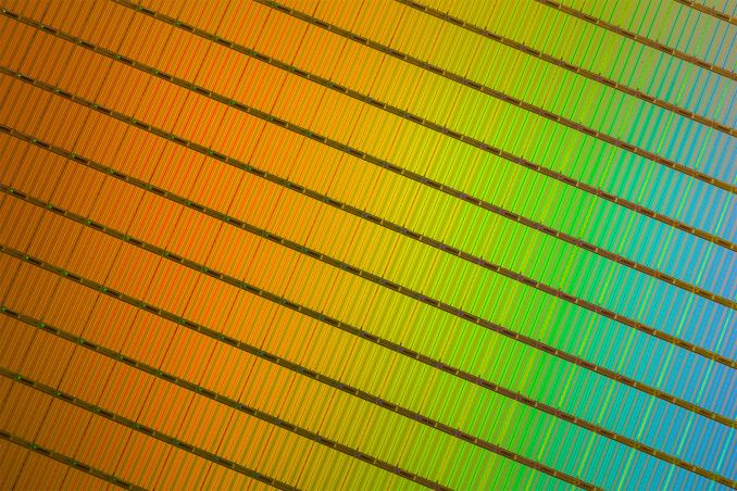
Yesterday Intel and Micron shared some new details of their 3D NAND technology and during the presentation they also showed a production wafer. I missed the wafer during the live broadcast (hence I couldn't include this in the initial write up), but fortunately Intel-Micron have now posted the recorded webinar, which I used to get a pretty good shot of the wafer. The quality isn't perfect, but it's good enough that I was able to make a fairly accurate estimation of the die size.
Disclaimer: The data and analysis presented in this article is based on estimations that are provided "as is" with no guarantee of full accuracy.

I calculated 19 dies vertically and 25 horizontally, which would yield a die size of 189.5mm. That's a bit too high since it doesn't take the partial dies on the edges of the wafer into account, so when taking that and the die cuttings (i.e. the space between dies) into account, my estimation of the die size would be 175mm. I think in reality it might be closer to 170mm, but I'll rather be conservative than present too optimistic numbers.
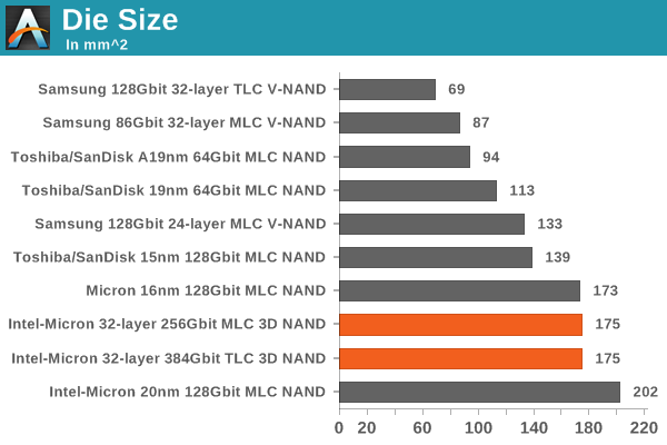
My die size estimation goes pretty well hand-in-hand with Intel-Micron's planar NAND dies. The two have never really focused on building small dies for mobile applications (e.g. microSD cards), which is why the die sizes are higher compared to the others with mobile focus. I was told Intel-Micron might build a smaller two-plane 3D NAND for mobile use if they see demand for it, but as I mentioned in yesterday's news post the initial die will be a 4-plane design that is aimed for SSDs.
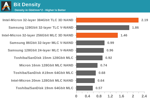
Now that we have the die size we can also estimate the most important metric i.e. the bit density. Intel-Micron's 32-layer 3D NAND design is by far more efficient than Samsung's, which is mostly explained by the much higher die capacity. The memory array efficiency (i.e. the portion of the die that's dedicated to memory cells) tends to scale with die capacity because the peripheral circuitry doesn't need too many modifications and thus the die area taken by the circuitry doesn't really increase with capacity.
I estimated Intel-Micron's 32-layer 3D NAND to have array efficiency of approximately 85%, which is very good and considerably higher than Samsung's 32-layer design (66% for the 86Gbit MLC part and 72% for the 128Gbit TLC part). Samsung did some peripheral circuitry optimizations for the 32-layer TLC part that explain the higher array efficiency versus the MLC part. When assuming similar array efficiencies for Intel-Micron and Samsung TLC dies, the bit densities are actually equivalent, suggesting that from a lithography and cell size perspective the two designs should be quite similar.
I now understand why Intel-Micron claim that their 3D NAND technology comes with disruptive cost because it really is the most efficient 3D NAND technology we have seen so far. It has twice the bit density compared to Micron's latest 16nm 128Gbit die, which should be enough to mitigate the higher production cost per wafer and make 3D NAND a natural successor to Intel-Micron's planar NAND. It will be interesting to see how Samsung's third generation V-NAND stacks up against Intel-Micron's 32-layer 3D NAND, but it's clear that Samsung must be able to increase the die capacity to remain competitive as it's more than just a game of layers.