
NVIDIA Formally Announces PCIe Tesla V100: Available Later This Year
Similar to last year, at this year's International Supercomputing Conference (ISC) NVIDIA has announced and detailed a PCI Express version of their latest Tesla GPU accelerator, the Volta-based V100. The conference itself runs from June 19 to 22, and with several speakers from NVIDIA scheduled for events tomorrow, NVIDIA is set to outline its next-generation efforts in HPC and deep learning with Volta.
With Volta discussed and described at their GPU Technology Conference in mid-May, NVIDIA upped the ante in terms of both features and reticle size: V100 is 815mm2 of custom TSMC 12FFN silicon, chock full of tensor cores and unified L1 cache per SM, along with many more fundamental – and as of yet not fully revealed – microarchitectural changes.
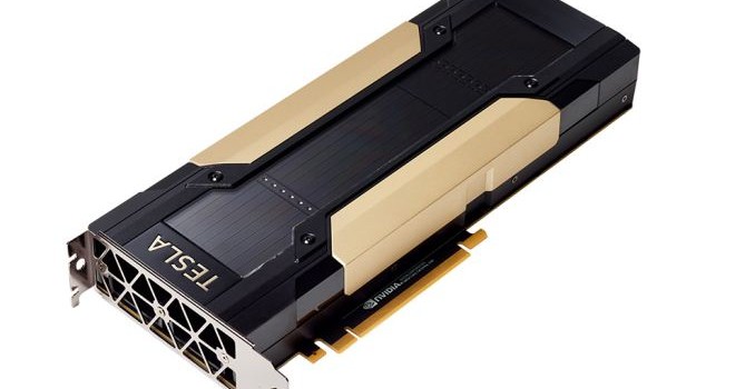
Like the previous Pascal iteration, the Tesla V100 PCIe offers a more traditional form factor as opposed to NVIDIA’s own mezzanine-type SXM2 form factor. This allows vendors to drop Tesla cards in traditional PCIe systems, making the cards far more accessible to server builders who don't want to build around NVIDIA's SXM2 connector or carrier board. The tradeoff being that the PCIe cards have a lower 250W TDP, and they don't get NVLink, instead relying on just PCIe.
| NVIDIA Tesla Family Specification Comparison | ||||||
| Tesla V100 (SXM2) |
Tesla V100 (PCIe) |
Tesla P100 (SXM2) |
Tesla P100 (PCIe) |
|||
| CUDA Cores | 5120 | 5120 | 3584 | 3584 | ||
| Tensor Cores | 640 | 640 | N/A | N/A | ||
| Core Clock | ? | ? | 1328MHz | ? | ||
| Boost Clock(s) | 1455MHz | ~1370MHz | 1480MHz | 1300MHz | ||
| Memory Clock | 1.75Gbps HBM2 | 1.75Gbps HBM2 | 1.4Gbps HBM2 | 1.4Gbps HBM2 | ||
| Memory Bus Width | 4096-bit | 4096-bit | 4096-bit | 4096-bit | ||
| Memory Bandwidth | 900GB/sec | 900GB/sec | 720GB/sec | 720GB/sec | ||
| VRAM | 16GB | 16GB | 16GB | 16GB | ||
| L2 Cache | 6MB | 6MB | 4MB | 4MB | ||
| Half Precision | 30 TFLOPS | 28 TFLOPS | 21.2 TFLOPS | 18.7 TFLOPS | ||
| Single Precision | 15 TFLOPS | 14 TFLOPS | 10.6 TFLOPS | 9.3 TFLOPS | ||
| Double Precision | 7.5 TFLOPS (1/2 rate) |
7 TFLOPS (1/2 rate) |
5.3 TFLOPS (1/2 rate) |
4.7 TFLOPS (1/32 rate) |
||
| Tensor Performance (Deep Learning) |
120 TFLOPS | 112 TFLOPS | N/A | N/A | ||
| GPU | GV100 (815mm2) | GV100 (815mm2) | GP100 (610mm2) | GP100 (610mm2) | ||
| Transistor Count | 21B | 21B | 15.3B | 15.3B | ||
| TDP | 300W | 250W | 300W | 250W | ||
| Form Factor | Mezzanine (SXM2) | PCIe | Mezzanine (SXM2) | PCIe | ||
| Cooling | Passive | Passive | Passive | Passive | ||
| Manufacturing Process | TSMC 12nm FFN | TSMC 12nm FFN | TSMC 16nm FinFET | TSMC 16nm FinFET | ||
| Architecture | Volta | Volta | Pascal | Pascal | ||
On the surface, the addition of tensor cores is the most noticeable change. To recap, tensor cores can be liked to a series of unified ALUs that are able to multiply two 4×4 FP16 matrices together and subsequently add that product to an FP16 or FP32 4×4 matrix in a fused multiply add operation, as opposed to conventional FP32 or FP64 CUDA cores. In the end, this means that for very specific kinds (and specifically programmed) workloads, Volta can take advantage of the 100+ TFLOPS capability that NVIDIA has tossed into the mix.
As for the specific specifications of the PCIe Tesla V100, it's similarly configured to the SXM2 version, getting the same number of CUDA cores and memory capacity, however operating at a lower clockspeed in-line with its reduced 250W TDP. Based on NVIDIA's throughput figures, this puts the PCIe card's boost clock at around 1370MHz, 85MHz (~6%) slower than the SXM2 version.
Interestingly, unlike the Tesla P100 family, NVIDIA isn't offering a second-tier PCIe card based on salvaged chips; so this generation doesn't have an equivalent to the 12GB PCIe Tesla P100. NVIDIA's experience with GP100/interposer/HBM2 assembly as well as continuing production of HBM2 has likely reduced the need for memory-salvaged parts.
Finally, PCIe-based Tesla V100 accelerators are “expected to be available later this year from NVIDIA reseller partner and manufacturers,” including Hewlett Packard Enterprise, which will offer three different PCIe Volta systems.