News


Unpacking AMD's Zen Benchmark: Is Zen actually 2% Faster than Broadwell?

Unpacking AMD’s Zen Benchmark: Is Zen actually 2% Faster than Broadwell?

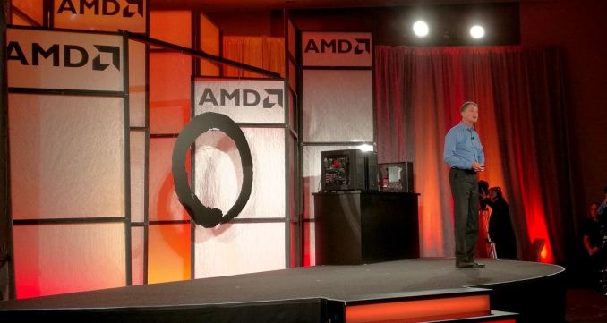
At a satellite event to Intel’s Developer Conference last week, AMD held an evening soiree with invited analysts and press to talk about their new upcoming Zen microarchitecture. This was intended to be a preview of tomorrow’s Hot Chips presentation, and we’ve already covered the juicier parts of the presentation in terms of microarchitecture announcements as well as diving deep into the Server-based Naples implementation and what the motherboards told us from memory and IO support. 

You can read both here:

AMD Zen Microarchitecture: Dual Schedulers, Micro-op Cache and Memory Hierarchy Revealed
AMD Server CPUs and Motherboard Analysis

There was one other element to the presentation that requires further discussion and analysis, if only to clean up some of the misinformation already present online and to label what was shown with a long list of potential caveats which most people seem to have passed by almost entirely. As part of the show, AMD compared the performance of their Zen engineering sample to an Intel Broadwell-E processor. 

In this test, they told the audience that each system was running eight cores, sixteen threads, and will all cores set to 3 GHz (implying no turbo). Memory arrangements were not disclosed, nor storage: we were told to assume comparable setups. 

We were too busy trying to decipher what was on screen (and take note of the results) to actually photograph the benchmark as it happened (there are videos online), but the benchmark they showed was Blender, an open source rendering engine, with a custom multithreaded workload. The test was to render a mockup of a Zen based desktop CPU, with an effective workload of 50 seconds for these chips. I’ve seen numerous reports about this result saying the difference was 1 or 2 seconds, but with rarely a mention of the benchmark length, which is as important. The overall results were

  Blender Time to Render / sec
Intel Broadwell-E
Core i7-6900K
8C / 16T
3 GHz all-core
49.05
AMD ZEN
Engineering Sample
8C / 16T
3 GHz all-core
48.07
(-0.98 sec, 1.998%)

All things being equal (we’ll get to that in a second), this would suggest that an 8-core AMD has a ~2% advantage over Broadwell-E at the same clock speeds. Despite this result, there are a lot of unverifiable parts to the claim which makes analysis of such a result difficult. I want to go through each of them one by one to ensure everyone understands what was presented. 

I’ll preface this analysis with two things though: one is that AMD was very careful in what they said at the event, and only said as much as they needed to. Thus is why the string of caveats for this benchmark test is fairly long. But also, AMD has to set expectations here: if they choose an environment and test that represents the peak, or relies on something special, users will feel burned again after Bulldozer. AMD has to temper those expectations but still represent a methodology that is effective to them. By leaving so many cards on the table, this can both be a help or a hindrance.

But given the measured and calm, professional nature of the event, as opposed to the wild and wacky AMD events of the past, it was clear (either by design or chance) that the words used said only as much as they needed to. Along with the microarchitecture discussions, it was designed to provide a good stepping stone on to the Hot Chips presentation a few days later.

So, caveats. Or disclaimers not readily provided. Let’s start at the top. 

1) The Results Are Not Externally Verifiable At This Time, As Expected

We were told the setups of the systems being used, but were unable to confirm the results manually. This is typically the case with a high level, early look at performance and other companies do this all the time.

This being said, it would look bad on reports if it to turns out or someone finds a chasm between pre-launch and launch data, so the aspect of reporting this data without understanding this caveat is fundamental. The basis of publishing scientific papers is repeatability and verification – while this wasn’t a scientific presentation, it is important to keep it in the back of your mind when you hear any benchmark numbers (AnandTech included – our numbers are designed to be verifiable and we want to have a history of honesty with our readers, especially when it comes to custom software/workloads we cannot disclose). 

2) No Memory or TDP Numbers Were Provided

We were able to determine that the AMD-based systems were running 2×8 GB of DDR4-2400, although we did not get a look at Intel’s memory arrangement. Similarly, due to the ES nature of the CPU, TDP numbers were also not shared however we did see all the AMD systems use either the AMD Wraith cooler (which is rated at 125W) or the new near silent cooler (95W). That tends to peg the system at a peak power consumption and some of AMD’s current competitive parts actually use a cooler designed for the bracket above in TDP (e.g. A10-7860K at 65W uses the 95W cooler, A10-7890K at 95W uses the 125W cooler). 

3) Blender Is an Open Source Platform

One of the issues of using open source is that the code is editable by everyone and anyone. Any user can adjust the code to optimize for their system and run a test to get a result. That being the case, it can be difficult to accurately determine the code base for this test, and is relatively impossible to determine the code base of Blender that was compiled for this test.

Even in the base code, there could be CPU vendor specific optimizations in either the code or compiler that influences how the code manipulates the cache hierarchy with the workload and adjusts appropriately. It also doesn’t help that Blender has elements in the code called ‘AMD’, which relates to a series of internal rendering features not related to the company. Going down the optimization for specific CPU microarchitectures leads on to another more philosophical issue…

4) Did It Actually Measure IPC? (The Philosophical Debate) 

In the purest sense, measuring the number of instructions per clock that a set of instructions can perform can determine the efficiency of a design. However, the majority of highly optimized code bases do not have general-purpose code – if it detects a particular microarchitecture it can manipulate threads and loops to take advantage of the code design. How should IPC be measured is the main question: using identical code bases makes it easier to understand but are often non-real-world compiler targets, or highly optimized code to show the best of what the processor can do (which means that IPC performance is limited to that benchmark)? With the results we saw, if the difference of about a second in just under fifty seconds translates into a 2% difference, is it accurate to say that this is a 2% IPC increase, or does it rely on optimized/non-optimized code? Optimizing code, or profiling compilers for specific code targets, is nothing new. In the holistic view, most analysts use SPEC benchmarks for this, as they are well-known code structures, even though most benchmarks are compiler targets – while SPEC is not particularly relevant for the real world workloads, it does give an indication about performance for unknown architectures/microarchitectures.

5) The Workload Is Custom 

One of the benefits of software like SPEC, or canned benchmarks like Cinebench, is that anyone (with a license) can pick up the workload and run with it. Those workloads are typically well known, and we can get performance numbers out that have known qualities in their interpretation. With a custom workload, that is not always the case. It comes down to experience – an unknown workload can have a lop-sided implementation of certain branches of code which is unknown when it comes to running the results. This is why rendering one scene in a film can take a vastly different time to another, yet the results for the ‘benchmark’ are significantly different depending on the architecture (one prefers lighting, another prefers tessellation etc.) Using known or standard workloads over long periods of time can offer insights into the results, whereas new workloads cannot, especially with so few results on offer.

6) It Is Only One Benchmark

There is a reason for AMD only showing this benchmark – it’s either a best case scenario, or they are pitching their expectations exactly where they want people to think. By using a custom workload on open source software, the result is very specific and cannot be extrapolated in any meaningful way. This is why a typical benchmark suite offers 10-20 tests with different workloads, and even enterprise standard workloads like SPEC come with over a dozen tests in play, to cater for single thread or multi-thread or large cache or memory or pixel pushing bottleneck that may occur. Single benchmarks on their own are very limited in scope as a result.

7) There’s Plenty about the Microarchitecture and Chip We Don’t Know Yet, e.g. Uncore

One of the more difficult elements on a processor is managing cross-core communication, as well as cross-core-cache snooping. This problem is overtly exponential, with the plausibility of more direct connections per core as the numbers go up. Intel has historically used a torus (ring) interconnect between cores to do this, with their large multi-core chips using a dual ring bus with communication points between the two. We suspect AMD is also using a ring bus in a similar methodology, but this has not been discussed at this time. There’s also the interconnect fabric between the cores and other parts of the chip, such as the Northbridge/Southbridge or the memory controllers. Depending on the test, the core-to-core communication and the interconnect can have different performance effects on the CPU. 

8) Clock Speeds Are Not Final, Efficiency Not Known

Performance of a CPU is typically limited by the power draw – there is no point getting a small amount of performance for a large increase in power such that efficiency has decreased. AMD has stated that power consumption and efficiency was a premier goal as this microarchitecture was developed.

At the demonstration, we were told that the frequency of the engineering samples was set at 3 GHz for all-core operation. We were told explicitly that these are not the final clock speeds, but it at the very least it puts the lower bound on the highest end processor. In reality, 3 GHz could be a walk in the park for the final retail units, depending on how much difference there is between the chips on display and what people will be able to buy. We are under the impression that the CPUs will have turbo modes involved, and those could be staggered based on the cores being used.

But this is why I said that 3 GHz is the lower bound of the high-end processor. We know from these results (assuming point 1 in this list) that the best processor from AMD will do at least 3 GHz. There’s no indication of power, and thus there’s no indication of efficiency either, which is also another important metric left in the ether.

9) We Will Have to Wait to Test

Everyone wants the next technology yesterday, so the ‘gimme gimme gimme’ feeling of new stuff is always there. AMD has already stated that general availability for Zen and Summit Ridge will be Q1, which puts the launch at four months away at a minimum. At this stage of the game, while AMD is trying to be competitive with Intel, they don’t want to generate too much hype and give the game away in case it goes incredibly pear-shaped. There’s the added element of the hardware and software being finalized or updated.

Since I’ve been reviewing, no CPU manufacturer has handed out review units four months before launch (in all honesty, we’re lucky to get a launch date sample a week in advance these days). In fact we’d have to go back to Nehalem and Conroe to find something that was sampled early; however Conroe just passed its 10th birthday and in that case, Intel knew they were on to a clear winner ahead rather than just ‘meeting expectations’. Also, early samples of a great product will mean users will wait for it to come out, which results in revenue loss (the Osborne effect) unless you have zero stock and/or an uncompetitive product that no-one is buying. In this decade, no x86 CPU manufacturer has offered samples this far out. I’d be more than happy for that to change and I would encourage companies to do so, but I understand the reasons why. 

Some Final Words

Much in the same way that taking an IQ test tells you how good you are at an IQ test, it is typically an indication that you are good/bad at other things as well (most well-engineered IQ tests go through a lot of spatial reasoning, for example). In this circumstance, a CPU performing a Blender test is only as good as a Blender test, but given what we know about the Zen microarchitecture, it is probably also good at other things. Just how good, in what metric and to what extent, is almost impossible to say.

AMD has given a glimpse of performance, and they’ve only said as much as they needed to in order to get the message across. However it has been up to the media to understand the reasons why and explain what those caveats are.

G.Skill Shows Off Trident Z 8x8 GB and 8x16 DDR4-3333 Memory Kits

G.Skill Shows Off Trident Z 8×8 GB and 8×16 DDR4-3333 Memory Kits

When Intel launched its new Core i7 Broadwell-E processors for high-end desktops earlier this year, all leading makers of motherboards released their new breed of Intel X99-based products that were supposedly ‘optimized’ for the new CPUs. Makers of memory modules are also beginning to roll-out their new DDR4 quad-channel kits that can operate at high frequencies with tight timings qualified for the new processors. At IDF this week, G.Skill demonstrated two new 64 GB and 128 GB kits designed for high-end workstations that require significant memory bandwidth.

G.Skill’s upcoming quad-channel Trident Z 64 GB (8×8 GB) memory kit is rated to run at 3333 MT/s with CL13 13-13-33 latency settings at 1.35 V. Right now, the company only offers quad-channel 64 GB DDR4-3333 kits with CL16 18-18-38 timings (albeit, these are either 4×16 GB or 8×8 GB kits). Another upcoming Trident Z quad-channel kit has 128 GB (8×16 GB) capacity and can operate at 3333 MT/s with CL14 14-14-34 timings, which is considerably better when compared to CL16 18-18-38 latencies of currently available 128 GB DDR4-3333 kits from the company.

G.Skill claims that the Trident Z kits it demonstrated at IDF are based on Samsung’s 8 Gb DDR4 chips, but does not reveal whether these are ICs made using 20 nm or sub-20 nm process technology. More advanced DDR4 ICs coupled with the new memory controller inside Intel’s Broadwell-E CPUs could allow G.Skill to build new 64 GB and 128 GB DDR4-3333 HEDT kits with tight timings. It is to be expected that the company has managed to cherry-pick the right previous-gen ICs for its new memory modules and depending on the binning of such ICs, prices will be high.

The demonstrations at IDF were conducted using two systems equipped with Intel Core i7-6800K processors and ASUS ROG Rampage V Edition 10 or ASUS X99-Deluxe II motherboards. The PCs were running basic applications and did not require extensive cooling.

Traditionally, all Trident Z kits come equipped with aluminum heatsinks and feature Intel XMP 2.0 SPD profiles to make it easier for end-users to run them at their data-rates with the right timings and voltage. Expect the same features from the kits that G.Skill demonstrated at IDF.

The manufacturer did not announce when it plans to release its new Trident Z 64 GB DDR4-3333 CL13 and Trident Z 128 GB DDR4-3333 CL14 kits as well as their prices. Right now, G.Skill’s fastest 128 GB DDR4-3200 CL16 is available for $730$1042, depending on the retailer. Memory prices tend to be exponential at the high end, so these will cost a lot more.

Supermicro Releases Intel Xeon Phi x200 (KNL) Systems: Servers and a Developer Mid-Tower

Supermicro Releases Intel Xeon Phi x200 (KNL) Systems: Servers and a Developer Mid-Tower

Supermicro has released two systems featuring Intel’s many-core Xeon Phi x200 processors: a workstation and an ultra-dense server. The platforms support up to 384 GB of DDR4 memory and are based on the good-old Intel C612 PCH. Due to high TDP of Intel’s Knights Landing CPUs, Supermicro had to use a custom closed-loop liquid cooling for its SuperWorkstation SYS-5038K-i.

Intel officially launched its Xeon Phi x200 many-core Knights Landing platform in June, but the company disclosed most of the details regarding its new processors last year at Supercomputing15. As discussed, every Xeon Phi x200 in LGA packaging has up to 72 cores (based on highly-modified Atom Silvermont microarchitecture) running at up to 1.5 GHz, with up to 36 MB of L2 cache, 16 GB of on-package high-performance memory (MCDRAM), six-channel DDR4 DRAM controller as well as 36 PCIe 3.0 lanes. The Xeon Phi x200 chips in LGA3647 form-factor can run as a host, directly with an operating system on board (including Windows Server 2016) which is an upgrade over the older Xeon Phi parts which only ran as co-processors on the PCIe bus. Moreover, the internal PCIe 3.0 root complex gives the Xeon Phi some PCIe lanes to allow other coprocessors to be plugged in – either additional Xeon Phi accelerators in the card form-factor, or AMD/NVIDIA cards, to maximize the compute horsepower.

SuperServer 5028TK-HTR

Since Intel Xeon Phi x200 processors are designed mainly for high performance computing, so as a result the OEM developers that build servers for customers tend to focus their efforts primarily on ultra-dense platforms.

One of the first Xeon Phi x200 solutions from Supermicro will be the SuperServer 5028TK-HTR, which packs four hot-swappable half-width nodes based on the company’s K1SPi motherboards into a 2U form-factor. Each 5028TK-HTR sports 12 3.5” hot-swappable SATA/SAS storage devices (three per node) as well as a 2000 W redundant PSU. Meanwhile, the K1SPi carries one P1 socket, six DDR4 DIMM slots (for up to 384 GB of DDR4), two PCIe 3.0 x16 low-profile slots, a PCIe 3.0 x4 slot, an Intel i350 dual port GbE controller, the Aspeed AST2400 BMC platform management.

Supermicro’s SuperServer 5028TK-HTR (as well as the K1SPi motherboard) support Intel Xeon Phi x200 processors with up to 250-260 W TDP. Machines supporting Knights Landing models featuring Omni-Path fabric will be announced at a later date.

SuperWorkstation 5038K-i

While HPC is a very important market for products like Xeon Phi, there is a segment of Xeon Phi clients who use them in desktop environments for financial analysis, oil and gas exploration, simulations as well as other applications. Also, HPC developers typically want a system-under-the-desk to actually develop their software with immediate results. Specifically for them, at the request of Intel, Supermicro introduced its SuperWorkstation 5038K-i desktop machine featuring the company’s K1SPE motherboard. The workstation is a self-contained unit sold complete, with CPU, DRAM, storage, PSU and cooling.

The chassis can fit in two 5.25” ODDs (or other peripherals), six 3.5″ and four 2.5” storage devices. The tower is equipped with multiple fans and come with one 750W power supply made by Seasonic as well as a custom-made closed-loop liquid cooling system with two 120 mm fans.

The K1SPE mainboard features one P1 socket (with eight-phase power delivery), six DDR4 DIMM slots (for up to 384 GB of DDR4), two PCIe 3.0 x16 slots, a PCIe 3.0 x4 slot, 10 SATA connectors, two GbE ports (via Intel i350), an IPMI LAN port, Aspeed AST2400 for graphics and management, USB 3.0 ports and so on. Despite the fact that the K1SPE uses regular ATX form-factor (with ATX12V and EPS12V power connectors), it will not be sold separately.

Both SuperServer 5028TK-HTR and SuperWorkstation 5038K-i machines should be available from Supermicro shortly, but only as complete systems. Therefore, their exact pricing could not be determined because it depends completely on exact configurations and quantity. We have been told that the workstation, the 5038K-i, is actually on back order with a number of customers already, however Supermicro is ramping up production as a result.

Additional from Ian: We’ve put in a request for a 5038K-i sample, which will run Windows Server 2016. As it’s a full x86 core (with additional VPUs), I want to see how well our regular x86 enterprise workloads translate into the Xeon Phi sphere. With a low single thread frequency but up to 72 cores, this test should be an interesting one.

Supermicro Releases Intel Xeon Phi x200 (KNL) Systems: Servers and a Developer Mid-Tower

Supermicro Releases Intel Xeon Phi x200 (KNL) Systems: Servers and a Developer Mid-Tower

Supermicro has released two systems featuring Intel’s many-core Xeon Phi x200 processors: a workstation and an ultra-dense server. The platforms support up to 384 GB of DDR4 memory and are based on the good-old Intel C612 PCH. Due to high TDP of Intel’s Knights Landing CPUs, Supermicro had to use a custom closed-loop liquid cooling for its SuperWorkstation SYS-5038K-i.

Intel officially launched its Xeon Phi x200 many-core Knights Landing platform in June, but the company disclosed most of the details regarding its new processors last year at Supercomputing15. As discussed, every Xeon Phi x200 in LGA packaging has up to 72 cores (based on highly-modified Atom Silvermont microarchitecture) running at up to 1.5 GHz, with up to 36 MB of L2 cache, 16 GB of on-package high-performance memory (MCDRAM), six-channel DDR4 DRAM controller as well as 36 PCIe 3.0 lanes. The Xeon Phi x200 chips in LGA3647 form-factor can run as a host, directly with an operating system on board (including Windows Server 2016) which is an upgrade over the older Xeon Phi parts which only ran as co-processors on the PCIe bus. Moreover, the internal PCIe 3.0 root complex gives the Xeon Phi some PCIe lanes to allow other coprocessors to be plugged in – either additional Xeon Phi accelerators in the card form-factor, or AMD/NVIDIA cards, to maximize the compute horsepower.

SuperServer 5028TK-HTR

Since Intel Xeon Phi x200 processors are designed mainly for high performance computing, so as a result the OEM developers that build servers for customers tend to focus their efforts primarily on ultra-dense platforms.

One of the first Xeon Phi x200 solutions from Supermicro will be the SuperServer 5028TK-HTR, which packs four hot-swappable half-width nodes based on the company’s K1SPi motherboards into a 2U form-factor. Each 5028TK-HTR sports 12 3.5” hot-swappable SATA/SAS storage devices (three per node) as well as a 2000 W redundant PSU. Meanwhile, the K1SPi carries one P1 socket, six DDR4 DIMM slots (for up to 384 GB of DDR4), two PCIe 3.0 x16 low-profile slots, a PCIe 3.0 x4 slot, an Intel i350 dual port GbE controller, the Aspeed AST2400 BMC platform management.

Supermicro’s SuperServer 5028TK-HTR (as well as the K1SPi motherboard) support Intel Xeon Phi x200 processors with up to 250-260 W TDP. Machines supporting Knights Landing models featuring Omni-Path fabric will be announced at a later date.

SuperWorkstation 5038K-i

While HPC is a very important market for products like Xeon Phi, there is a segment of Xeon Phi clients who use them in desktop environments for financial analysis, oil and gas exploration, simulations as well as other applications. Also, HPC developers typically want a system-under-the-desk to actually develop their software with immediate results. Specifically for them, at the request of Intel, Supermicro introduced its SuperWorkstation 5038K-i desktop machine featuring the company’s K1SPE motherboard. The workstation is a self-contained unit sold complete, with CPU, DRAM, storage, PSU and cooling.

The chassis can fit in two 5.25” ODDs (or other peripherals), six 3.5″ and four 2.5” storage devices. The tower is equipped with multiple fans and come with one 750W power supply made by Seasonic as well as a custom-made closed-loop liquid cooling system with two 120 mm fans.

The K1SPE mainboard features one P1 socket (with eight-phase power delivery), six DDR4 DIMM slots (for up to 384 GB of DDR4), two PCIe 3.0 x16 slots, a PCIe 3.0 x4 slot, 10 SATA connectors, two GbE ports (via Intel i350), an IPMI LAN port, Aspeed AST2400 for graphics and management, USB 3.0 ports and so on. Despite the fact that the K1SPE uses regular ATX form-factor (with ATX12V and EPS12V power connectors), it will not be sold separately.

Both SuperServer 5028TK-HTR and SuperWorkstation 5038K-i machines should be available from Supermicro shortly, but only as complete systems. Therefore, their exact pricing could not be determined because it depends completely on exact configurations and quantity. We have been told that the workstation, the 5038K-i, is actually on back order with a number of customers already, however Supermicro is ramping up production as a result.

Additional from Ian: We’ve put in a request for a 5038K-i sample, which will run Windows Server 2016. As it’s a full x86 core (with additional VPUs), I want to see how well our regular x86 enterprise workloads translate into the Xeon Phi sphere. With a low single thread frequency but up to 72 cores, this test should be an interesting one.