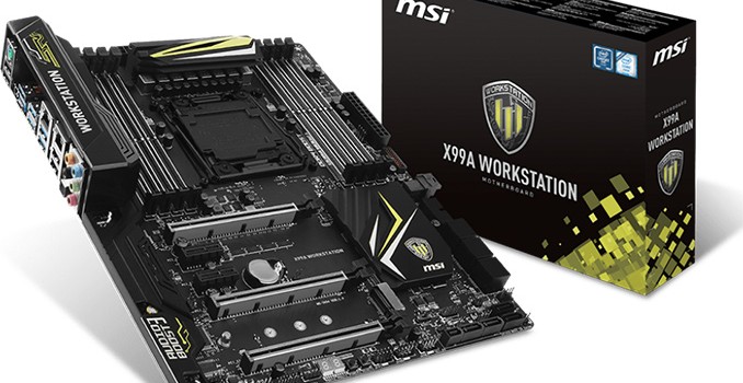
MSI Unveils the X99A Workstation Motherboard
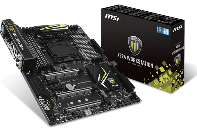
Last week MSI introduced its new X99A Workstation motherboard, part of the X99 refresh we’ve seen over the past couple of months following the launch of the Broadwell-E processor line. Despite the name ‘workstation’, this board is based on the consumer-grade Intel X99 PCH rather than the server oriented parts, and as a result it supports overclocking. Part of the ‘Workstation’ feature set means that it has qualified support for NVIDIA Quadro PCIe cards, compatibility with ECC memory, and a U.2 connector for storage. The manufacturer claims that the mainboard uses special components that can improve the endurance of the board, although the warranty is still listed as three years.
Typically, workstation-class motherboards for Intel Xeon E5 v3/v4 processors in LGA2011-3 packaging are based on the Intel C612 PCH, which has the same I/O features as the desktop-class Intel X99, but also supports a number of additional capabilities, which are important for business environments, such as vPro, RSTe, SVT and so on (you can read more about Intel’s 612 chipset here). When it comes to professional workstation vendors that supply machines to large corporations, those technologies make a lot of sense and are generally welcome. However, for prosumers and for many professionals working in small/medium businesses, these options might not be required, which is why a lot of motherboard manufacturers offer Intel X99-based workstation-class mainboards that fully support overclocking but continue to have numerous workstation features (such as support for ECC, when Xeon CPUs are installed). This is the focus of the X99A Workstation.
The MSI X99A Workstation (7A54) motherboard features one LGA2011-3 slot for Intel Core i7 as well as Intel Xeon E5 processors, though it is interesting to note that the maker does not list Intel Xeon SKUs in its qualified vendor list. Along with the eight-phase power delivery (which uses solid-state chokes), the mainboard carries eight DDR4 memory slots that not only support non-ECC/unbuffered memory modules with XMP 2.0 (and up to DDR4-3333 supported in OC modes), but also RDIMMs with ECC with applicable CPUs.
For add-in cards, the motherboard has three PCIe 3.0 x16 slots (which can work in x16, x16/x16, x8/x16/x8 modes with CPUs featuring 40 PCIe lanes) as well as two PCIe 2.0 x1 slots from the chipset.

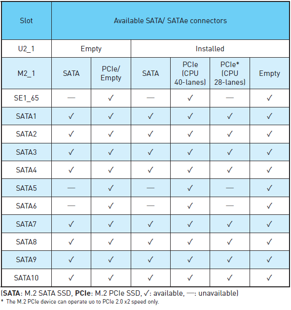
When it comes to storage-related capabilities, the MSI X99A Workstation comes with one M.2-22110 slot, one U.2 port running in PCIe 3.0 x4 mode, and a SATAe port (unavailable when M.2 and U.2 are used). For traditional HDDs/SSDs/ODDs, the motherboard offers 10 SATA 6 Gb/s ports (including two ports from SATAe). So, in total the motherboard can support up to 12 storage devices.
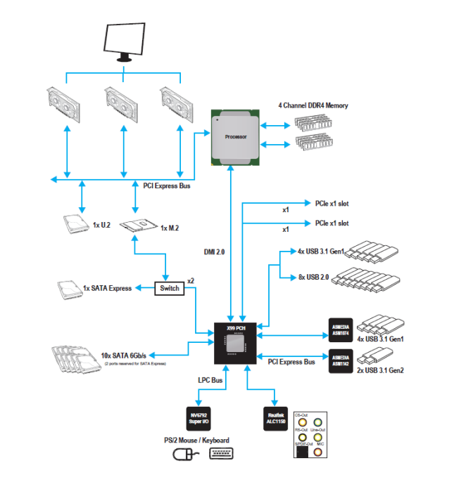
The chipset diagram shows what is in play, and the M.2 configuration is a little odd given that 2 lanes come from the PCH and another two from the CPU despite standard CPU bifurcation stops at x4. In this instance I would have suggested that MSI merely considers the M.2 a CPU device with x4, given that the system would support it, but because Intel has 28-lane CPUs for the platform this can cause differences in bandwidth available. MSI shared the storage support matrix to help users looking into the X99A Workstation:
For audio and networking, the MSI X99A Workstation uses the Realtek ALC1150 solution (with PCB separation and filter caps) with 7.1-channel analog as well as S/PDIF outputs. For networking, the motherboard has an Intel I218LM and an Intel I210AT Gigabit LAN controllers, with teaming support listed. The mainboard also features ASMedia’s ASM1142 controller to enable one USB 3.1 Type-C (10 Gbps) and one USB 3.1 Type-A (10 Gbps) connectors on the rear panel. In addition, the motherboard supports eight USB 3.1 Type-A (5 Gbps) and eight USB 2.0 ports.
The MSI X99A Workstation should be available shortly, but pricing has not yet been decided.