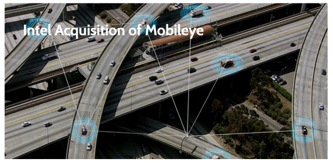
Intel to Acquire Mobileye for $15 Billion
In an interesting announcement today, Intel and Mobileye have entered into an agreement whereby Intel will commence a tender offer for all issued and outstanding ordinary shared of Mobileye. At $63.54 per share, this will equate to a value of approximately $15 billion.
Mobileye is currently one of a number of competitors actively pursuing the visual computing space, and the high item on that agenda is automotive. We’ve seen Mobileye announcements over the last few years, with relationships with car manufacturers on the road to fully autonomous vehicles. Intel clearly wants a piece of that action, aside from its own movement into automotive as well as cloud computing required for various automotive tasks.
Intel estimates that vehicle systems, data, and the services market for automotive to have a value around $70 billion by 2030, including edge cases through backhaul into cloud. This includes predictions such that 4TB of data per day per vehicle will be generated, which is going to require planning in infrastructure. Intel’s expertise in elements such as the RealSense technology and high-performance general compute will be an interesting match to Mobileye’s portfolio.
“This acquisition is a great step forward for our shareholders, the automotive industry, and consumers,” said Brian Krzanich, Intel CEO. “Intel provides critical foundational technologies for autonomous driving including plotting the car’s path and making real-time driving decisions. Mobileye brings the industry’s best automotive-grade computer vision and strong momentum with automakers and suppliers. Together, we can accelerate the future of autonomous driving with improved performance in a cloud-to-car solution at a lower cost for automakers.”
The acquisition will combine into a single organization under Intel’s Automated Driving Group, to be HQ in Israel and led by Prof Shashua, Mobileye’s co-founder, Chairman and CEO. All current contracts under Mobileye for automotive OEMs and tier-one suppliers will be retained under the single group, which will also be under Doug Davis, Intel’s SVP of Intel’s Automotive.
Mobileye currently offers on its roadmap products such as the EyeQ4 and EyeQ 5 SoCs, for level 3/4 autonomy in 2018 and 2020 respectively, as well as high-performance FPGAs for vision analytical techniques. The acquisition of Altera by Intel over a year ago as a step into the FPGA market may come into play here, as well as Intel’s semiconductor manufacturing facilities. As with Altera, it will likely take some time before full integration between Intel’s resources and Mobileye’s technology occurs.
There will be an investor call webcast on 3/13 at 8:30 am (ET) about this announcement at this link here. The full transaction is expected to close within nine months, subject to regulatory approval, and is not subject to any financing conditions. Intel intends to fund the acquisition with cash from the balance sheet.
As we get more information we will let you know.
Additional 1: For scope, Intel’s purchase of Altera was $16.7 billion, as we reported here.
Additional 2: Here is the Investor Call slide deck.


Additional 3: It will require purchasing 95% of the ordinary stock, and will use offshore cash that Intel has not repatriated into the US.