Vik


Qualcomm Announces Snapdragon Wear 2100 IoT SoC

Qualcomm Announces Snapdragon Wear 2100 IoT SoC

Along with today’s announcements of the Snapdragon 425, 435 and 625, we also see the reveal of a new wearables-oriented SoC: the Snapdragon Wear 2100. In the past we’ve seen vendors use low-end smartphone SoCs such as the Snapdragon 400 (Motorola Moto 360 2nd gen). In fact, to date only Samsung (Exynos 3250) and Apple (S1) were able to employ chipsets that were specifically designed for wearables. This was rather unfortunate for other wearable vendors as devices such as smartwatches require much higher efficiency and lower power than what “off-the-shelf” SoCs were able to offer. Qualcomm sees to fix this by introducing a new lineup of chips called Snapdragon Wear that are designed with wearables in mind. 

The Snapdragon Wear 2100 is a quad-core Cortex A7 running at up to 800MHz or 1.2GHz (Qualcomm at various points states both) with an Adreno 304 GPU and 400MHz LPDDR3. The choice of using a Cortex A7 is warranted by the fact that Cortex A53s are too power hungry for wearables and that it’s likely too early to see Cortex A35 based SoCs as ARM announced the core only a couple of months ago. A big advantage that Qualcomm has with the Wear 2100 is that it’s able to offer an integrated X5 modem for basic cellular connectivity (Supporting all current standards). 

With the Wear 2100 Qualcomm is now able to offer a fitting SoC for wearable devices and it’s very likely that consumers will see direct benefits such as improved battery life. Qualcomm hasn’t specified any availability for the SoC but discloses that there are multiple devices in development using the processor.

Qualcomm Announces Snapdragon 625, 425 & 435 Mid- and Low-End SoCs

Qualcomm Announces Snapdragon 625, 425 & 435 Mid- and Low-End SoCs

Today Qualcomm announced three new SoCs in the mid and low-end Snapdragon lineup. At the lowest end we find the Snapdragon 425 offering a very frugal CPU configuration consisting of 4x Cortex A53’s clocked in at 1.4GHz. The chipset is aimed at replacing the Snapdragon 410 and 412 and improves on them with an upgrade on the modem block as well as media decoder and encoder capabilities, now enabling 1080p HEVC decode and encode.

The Snapdragon 435 replaces the Snapdragon 430 which was only announced just a few months ago and also sees an improvement in the modem block used as we see it now going from UE Category 4 to UE Category 7. On the CPU side we see a 200MHz boost in the frequency of the faster of the two quad-core A53 clusters, now reaching 1.4GHz. In both the Snapdragon 425 and 435 we don’t see a change in the GPU but it’s possible clocks have changed; unfortunately details on the matter are still sparse. Both the Snapdragon 425 and 435 are manufactured on a “28nm LP” process but sadly it wasn’t specified which foundry is manufacturing them.

New 2016 Mid & Low-End Snadpragons
SoC Snapdragon 425
(MSM8917)
Snapdragon 435
(MSM8940)
Snapdragon 625
(MSM8953)
CPU 4x A53 @ 1.4GHz 4x A53 @ 1.4GHz

4x A53 @ ? GHz

4x A53 @ 2.0GHz

4x A53 @ ? GHz

Memory 1x 32-bit @ 667MHz
LPDDR3

5.3GB/s b/w

1x 32-bit @ 800MHz
LPDDR3

6.4GB/s b/w

1x 32-bit @ 933MHz
LPDDR3

7.45GB/s b/w

GPU Adreno 308 Adreno 505 Adreno 506
Encode/
Decode
1080p
H.264 & HEVC (Decode)
2160p
H.264 & HEVC (Decode)
Camera/ISP Dual ISP
16MP
Dual ISP
21MP
Dual ISP
24MP
Integrated
Modem
“X6 LTE” Cat. 4
150Mbps DL 75Mbps UL

2x20MHz C.A. 
(DL & UL)

“X8 LTE” Cat. 7
300Mbps DL 100Mbps UL

2x20MHz C.A. 
(DL & UL)

“X9 LTE” Cat. 7
300Mbps DL 150Mbps UL

2x20MHz C.A. 
(DL & UL)

Mfc. Process 28nm LP 14nm LPP

Most importantly comes the announcement of the Snapdragon 625. This is the successor to the Snapdragon 617 which along with the 615 has seen quite a lot of success in mid-range and budget smartphones. The CPUs remain two quad-core clusters of Cortex A53’s but now the performance cluster is clocked at up to 2GHz representing a large increase to the 1.5GHz SoCs which the 625 is replacing. The GPU has also been upgraded from an Adreno 405 to a newer generation Adreno 506. The modem again has seen a slight upgrade from an X8 to an X9 block, allowing for an increase in the uplink performance if the network supports it.

The biggest surprise out of today’s announcements is the fact that the Snapdragon 625 is manufactured on Samsung’s/GlobalFoundry’s 14nm LPP process. Qualcomm thus is the first vendor to announce a non-high-end SoC to use a new FinFET manufacturing process which is quite astonishing as I hadn’t expected vendors be able to do the migration so early on in the technology’s lifetime, which may be a positive indicator that we might be seeing FinFET adopted across the mid-range earlier than expected.

The new SoC should be sampling to vendors in mid-2016 with availability in commercial devices in the second half of 2016.

EVGA Begins Selling "VR Edition" GeForce GTX Video Cards for VR Gaming Rigs

EVGA Begins Selling “VR Edition” GeForce GTX Video Cards for VR Gaming Rigs

EVGA this week began to sell their GeForce GTX 980 Ti VR Edition video cards, a new lineup tailored for those who plan to use a virtual reality headset. The graphics boards are equipped with an internal HDMI port and a special adapter for 5.25-inch bay that simplifies plugging VR headsets to PCs.

The family of EVGA’s VR Edition graphics cards currently includes two models, both of which are modifications of EVGA’s existing GTX 980 Ti card designs. The first VR Edition card is the EVGA GeForce GTX 980 Ti VR Edition Gaming ACX 2.0+ (06G-P4-3996), which uses the company’s own ACX 2.0+ cooler featuring 8-mm copper heatpipes, aluminum radiators, two fans and a memory/MOSFET cooling plate,  while the second is the EVGA GeForce GTX 980 Ti VR Edition Gaming (06G-P4-3998), which uses NVIDIA’s reference cooler for high-end boards. As these are GTX 980 Ti cards, both cards are based on the GM200 GPU with 2816 stream processors, 176 texture units, 96 ROPs as well as a 384-bit memory bus. The GPUs are clocked at 1000 MHz/1076 MHz (base/boost), whereas the attaced 6 GB of GDDR5 memory is clocked at 7 Gbps.

A brief examination of the pictures provided on EVGA’s website indicates that both VR Edition graphics cards are using PCBs that resemble NVIDIA’s reference designs for the GeForce GTX 980 Ti/Titan X (8pin + 6pin power inputs), but they feature an important addition. The adapters have an internal HDMI 2.0 port that connects to a special adapter for 5.25-inch bay that has an HDMI output as well as two USB 3.0 connectors. The adapter is designed to connect the Oculus Rift, the HTC Vive or any other VR headset to a PC without using ports on the backside of the computer, which makes the process considerably more comfortable.

EVGA’s product literature indicates that they’re primarily focused on first-time buyers – those who will be building or upgrading systems ahead of the spring VR headset launches – as these headsets will be launching some time before any 16nm high-end GPUs. That said, I wouldn’t be surprised if the VR Edition cards also proved popular with gamers who already have a PC powered by the GeForce GTX 980 Ti and are looking forward to build a multi-GPU system to play VR games, as VR SLI scaling is looking optimisitc thanks to the ability to forgo AFR and assign a GPU to each eye.

From a design perspective, routing HDMI port to the backside of the card should be relatively easy. EVGA hasn’t released any board shots, but they likely only had to slightly modify voltage regulating module of their GeForce GTX 980 Ti boards without any significant changes to its design. Consequently I wouldn’t be surrprised if other makers of video cards do something similar later on – the idea seems rather obvious in hindsight – though for the moment EVGA is the first and only game in town. Perhaps, if VR gaming takes off in the next year or two, AMD and NVIDIA could add internal graphics ports to their reference designs.

Both EVGA GeForce GTX 980 Ti VR Edition graphics cards are available now for $699, which comes at around a $70 premium over their normal reference-clocked GeForce GTX 980 Ti boards (usually $620 – $630). As it appears, VR gamers will have to pay a extra for the VR adapter for 5.25” bays. However, given the additional comfort, it may well worth the investment, especially for those who plan on frequently plugging and unplugging VR headsets (or for that matter even tradtional HDMI displays).

The Lenovo Ideapad Y700 Laptop Review

The PC gaming market has been pretty strong market over the last couple of years, and recent developments have pushed the boundaries again. With launches of virtual reality headsets, we’ve seen even notebook manufacturers getting prepared to dri…

Plextor Introduces M6S Plus SSDs with Toshiba’s 15nm MLC NAND

Plextor Introduces M6S Plus SSDs with Toshiba’s 15nm MLC NAND

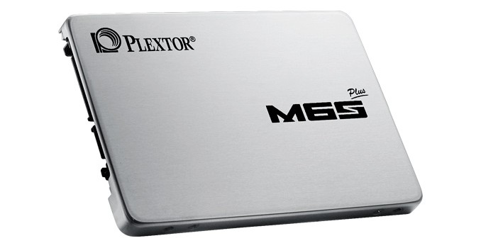
Plextor this week introduced its M6S Plus SSDs that use Toshiba’s latest MLC NAND flash memory as well as a proven controller from Marvell. The new SSDs offer the same level of performance and the same feature set as their predecessors, the M6S drives introduced in 2014. The drives offer read and write speeds expected from SATA SSDs as well as Plextor’s technologies designed to guarantee high reliability and high performance after long periods of usage.

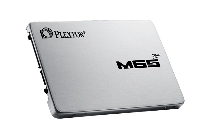
The new Plextor M6S Plus SSDs are based on the Marvell 88SS9188 controller as well as Toshiba’s newest 15 nm MLC NAND. Earlier Plextor offered M6S solid-state drives based on the same controller chip, but featured Toshiba’s older 19 nm MLC NAND. Apparently, Plextor will have to switch to a new type of NAND as manufacturers tend to decrease production of memory using outdated process technologies. The new drives are offered in 2.5-inch/7 mm form-factor and use the SATA-6 Gb/s interface.

The Plextor M6S Plus SSDs feature 128 GB, 256 GB and 512 GB capacities. They are rated to offer maximum sequential read/write speed of up to 520/440MB/s. Maximum random 4K read/write speed declared by Plextor is 94K/80K IOPS (input/output operations per second). It is noteworthy that to guarantee high performance, the new SSDs from Plextor are equipped with up to 768 MB of DDR3 DRAM-based cache.

Specifications of Plextor M6S Plus SSDs
  PX-128M6S+ PX-256M6S+ PX-512M6S+
Capacity 128 GB 256 GB 512 GB
Controller Marvell 88SS9188
NAND Toshiba, MLC 15nm
Cache 256 MB DDR3 512 MB DDR3 768 MB DDR3
Sequential Read Speed up to 520 MB/s up to 520 MB/s up to 520 MB/s
Sequential Write Speed up to 300 MB/s up to 420 MB/s up to 440 MB/s
4K Random Read up to 88K IOPS up to 90K IOPS up to 94K IOPS
4K Random Write up to 75K IOPS up to 80K IOPS up to 80K IOPS
Form-Factor 2.5-inch/7mm
Interface SATA-6 Gbps

Notably, the performance specifications for the new M6S Plus lineup is identical to that of the previous M6S series. As Plextor didn’t switch controllers and didn’t switch NAND vendors, this means that they most likely are just using 15nm NAND as a drop-in replacement for their existing designs, and there won’t be any generational performance changes such as using fewer, higher capacity NAND dies. This has been an issue in the past when vendors have switched to newer generation NAND and labeled the resulting product under an old brand, so kudos to Plextor for making the 15nm drives their own line anyhow.

However while the switch to 15nm NAND doesn’t impact performance, it’s unclear whether the endurance of the newer M6S Plus series has been impacted, as the company hasn’t published any endurance figures for the new drives. Typically, MLC NAND produced using thinner fabrication process has lower P/E cycle rating compared to flash memory produced using thicker manufacturing technology. The 19nm M6S series was rated for 72TB, so it will be interesting to see where the M6S Plus ends up.

Moving on, contemporary Plextor’s SSDs also ship with the company’s PlexTurbo RAM caching technology, which is aimed to improve performance beyond limitations of SATA-6Gb/s interface. The caching works like RAM disk, hence, uses system memory. The M6S Plus also supports TrueSpeed (supposed to guarantee maximum performance over long usage periods) and TrueProtect (a multi-layer error correction capability) firmware-based technologies developed by the company.

Finally, exact MSRPs of the Plextor M6S Plus drives are unknown. However, Amazon plans to start selling the 128 GB version for $62, the 256 GB model for $91 and the 512 GB flavour for $166 shortly.

The Plextor M6S Plus SSDs appear to be pretty affordable, in fact, even more affordable than their predecessors. Apparently, the recent price drops of NAND flash helped Plextor to build inexpensive SSDs based on 15 nm MLC NAND flash from Toshiba, which is not a bad choice, considering the fact that the company managed to maintain performance numbers of the M6S. By contrast, many of Plextor’s rivals are using TLC NAND to make cheap SSDs.