News


Understanding Brightness in AMOLED and LCD Displays

Understanding Brightness in AMOLED and LCD Displays

While we generally avoid going into deep detail when it comes to our display testing, in light of statements that seemingly contradict our testing it becomes important to contextualize our display tests. Many people are often confused by contradicting statements regarding the peak brightness of an AMOLED display, as we will state that the Samsung Galaxy Note 4’s display reaches a maximum of 462 cd/m^2, while other sites often state that the Note 4’s display reaches a maximum of 750 cd/m^2. Another commonly cited discrepancy is that we rate the Nexus 6’s display to reach a peak brightness of 258 nits, while others have rated the Nexus 6’s display to be as bright as 400 nits.

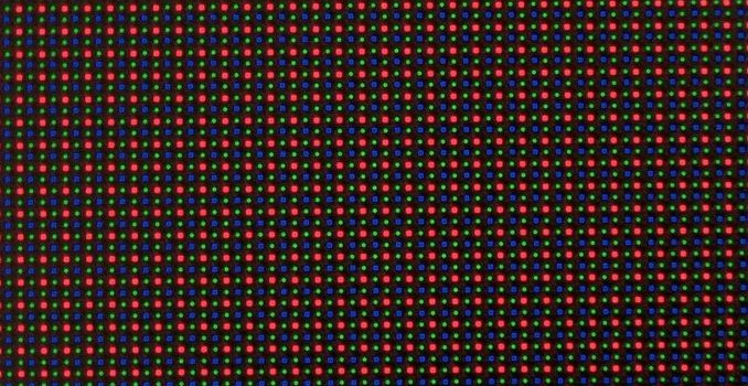
One might immediately assume that one measurement is right, and the other is false. In truth, both measurements are achievable, as we’ll soon see. Before we get into any discussion of testing methodology though, we must first understand how AMOLED and LCD displays work. Fundamentally, LCD and OLED displays are almost completely different from one another, but face similar issues and limitations. LCD is the older of the two technologies, and is fundamentally quite simple, although not quite as simple as OLED. In short, we can view an LCD display as made of a backlight, and a color filtering array which has liquid crystals that control the passage of light, along with polarizers to make sure that the filtering system works correctly.

An Apple iPod Touch music player disassembled to show the array of white-edge LED’s powered on with the device / ReTheCat

To break this system down further, we can look at the backlight. In the case of mobile devices, the only acceptable backlight system for thickness and power efficiency reasons is the edge-lit LED, which places a line of LEDs along an edge of the display, which is then diffused through a sheet of transparent material with strategically-placed bumps in the material to create points of light via total internal reflection. For the most part, LEDs in use today are blue LEDs with yellow phosphors in order to increase efficiency, although this means that the natural white point of such a backlight is higher than 6504k and requires filtering in order to reach a calibrated white point.

Schematic diagram IPS LC display / BBCLCD

While the backlight is relatively simple, the actual color filtering is a bit more complicated, although we will avoid extensive depth in this case. In the case of IPS, the structure is generally quite simple in nature, with two electrodes in plane with each other, which is used to generate an electric field that rotates the orientation of the liquid crystals in plane with the display to dynamically alter the polarization of the light that can pass through the liquid crystal array. With a set of fixed polarizers before and after the liquid crystal array, by using the controlling TFTs to alter the voltage applied on the electrodes one can adjust individual color output on a per-pixel basis.

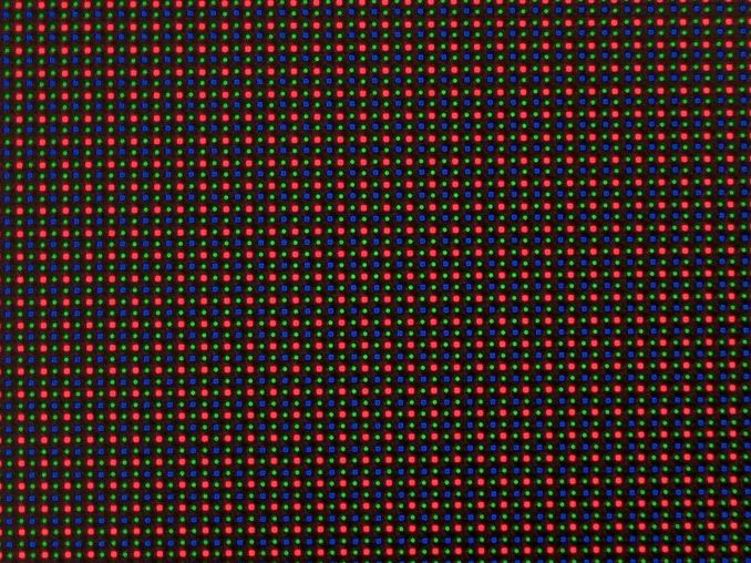
Schematic of a bilayer OLED: 1. Cathode (−), 2. Emissive Layer, 3. Emission of radiation, 4. Conductive Layer, 5. Anode (+) / Rafał Konieczny

AMOLED is a fundamentally different approach to the problem, which uses organic emitters deposited upon a substrate. These emitters are designed to emit red, green, or blue when voltage is applied across two electrodes. Similarly, TFTs are needed to control each pixel. As one can see, AMOLED is a simpler solution, but in practice the issues with such an implementation can be quite complex.

In order to determine what picture content to use for a measurement of maximum brightness, we must turn to a measurement known as Average Picture Level (APL). This is best explained as the percentage of the display that is lit up compared to a full white display, so a display that is completely red, green, or blue would be 33% APL.

As one might already be able to guess, with AMOLED power consumption is highly dependent upon the content displayed. With a pure white image, every pixel must be lit, while with a pure black image every pixel is off. As the display typically has a maximum power use set for a mobile device, this opens up the capability for AMOLED displays to allocate more power per pixel (i.e. higher maximum luminance) when not displaying a full-white image. This is in contrast with the edge-lit LCDs used in mobile displays, which have relatively limited local-dimming capabilities. As a result, the maximum brightness of an LCD is relatively fixed, regardless of the displayed content.

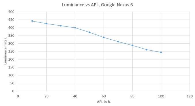
In the case of the Nexus 6, we can clearly see dimishing returns after 40% APL as there is efficiency droop on AMOLED displays that are similar in nature to LED backlights. While now it’s easy to understand why it is that AMOLED can vary in maximum brightness, the question is which brightness is “correct”. While an AMOLED display can technically have a maximum brightness of 750 nits, it’s unlikely that people will look at images effectively equivalent to 1% of the display lit up with white.

In practice, it turns out that with Lollipop and almost all web pages, the average picture level is quite high. It’s increasingly rare to see cases where displayed content is below 50% APL. According to Motorola, 80% APL represents an average APL for light UIs and in light of this, it seems appropriate to test at similarly real-world APLs. Taking a look at some commonly used applications in Lollipop, we see that the APL is regularly at or above even Motorola’s 80% figure. I opened some of the applications on my Nexus 6’s homescreen to take screenshots of whatever they had open when they came up, and I’ve tabulated the results below.

  APL in %
Messenger 86
Calculator 49
Settings 84
Calendar 80
Phone 89
Reddit Is Fun (Light) 77
Reddit Is Fun (Dark) 23
Chrome New Tab 86
Wikipedia 83
AnandTech 52
AnandTech Article 81
Twitter 76

As you can see, many of the screens in Android’s interface as well as web pages and third party apps have a high APL. There are exceptions, like the Calculator application and any application with a dark theme, but the overall trend is clear. Google’s new interface style also means that applications are more likely to adopt interfaces with large amounts of white than in the past. 

As a result of this, we test at 100% APL in order to get an idea of perceived brightness. While there may be some need for lower APL testing, it’s important to also consider cases such as OLED aging which will lower peak brightness over time. It’s also important to consider that the delta between 80% APL and 100% APL in this case is around 44 nits. This makes for about an 18% delta in brightness, which ends up being around the noticeable difference in most cases. While our testing is subject to change, in the case of brightness we currently do not see much need to dramatically alter our methodology.

Crossbar's Resistive RAM Technology Reaching Commercialisation Stage

Crossbar’s Resistive RAM Technology Reaching Commercialisation Stage

While the first 3D NAND chips have just found their way to the market and most NAND manufacturers are still developing their designs, there are already a handful of next generation memory technologies in development that are slated to supersede NAND in the next decade or so. One of the most promising technologies is Resistive Random Access Memory, which is more commonly referred to as Resistive RAM or just RRAM. Similar to NAND, RRAM is non-volatile, meaning that it will retain data without power unlike regular DRAM, which needs a continuous power source. Multiple companies are developing RRAM including semiconductor giants like Samsung and SanDisk, but Crossbar, a US based startup, has probably the most advanced design so far.

I’ve been following Crossbar for quite some time, but I haven’t written anything about the company until now. The company was founded in 2010, headquarters in Santa Clara, California and has secured over $50 million in funding. The company’s roots come from the University of Michigan and its Chief Scientist and co-founder, Prof. Wei Lu, is currently an associate professor at the university. The Crossbar team consists of 40-45 members at this point, of which most have extensive backgrounds in semiconductor research and development. 

The big benefits RRAM have over NAND are performance and endurance. NAND read latencies are typically in the order of hundreds of microseconds, whereas Crossbar claims latency of as low as 50 nanoseconds for its RRAM design. Endurance in turn can be millions of program/erase cycles, although for the early designs Crossbar is aiming at more conservative ~100K cycles. 

Last week at IEDM Crossbar announced that it is now entering the commercialization stage. In other words, it has already shown a working silicon and it has also proved that the design can be transferred to commercial fab for high volume manufacturing, so the company is now working with the fabs to build final products.

At first Crossbar is aiming at the embedded market and is licensing its technology to ASIC, FPGA and SoC developers with first samples arriving in early 2015, and mass production scheduled for late 2015 or early 2016. Aside from licensing, Crossbar is also developing standalone chips with higher capacity and density, which should enter the market about a year after the embedded RRAM designs (i.e.most likely sometime in 2017).

The beauty of RRAM is that it can be manufactured using a regular CMOS process with only a few modifications. NAND and especially 3D NAND require expensive special tools (for things like high aspect ratio etching), which is why only a handful of companies are making 3D NAND. RRAM in turn can be manufactured by practically any existing fab with very little added cost, which ultimately results in lower prices due to more competition.

Additionally, RRAM doesn’t share NAND’s lithography issues. As we know, the sole reason why 3D NAND was invented is because planar NAND can’t really scale below 15nm without serious endurance and performance considerations. However, RRAM can efficiently scale to 4-5nm without any issues and in fact Crossbar has already demonstrated an 8nm chip that it built in its R&D labs (most likely using multiple patterning). Moreover, RRAM can be stacked vertically to create a 3D crosspoint array for increased density and so far Crossbar is at three layers, but first commercial standalone chips are expected to feature 16 layers and up to 1Tbit capacity. 

Obviously, there are still several hurdles to cross before RRAM is ready to challenge NAND, but it’s good to hear that there has been significant progress in development and the technology has gained interest from the fab companies. Faster, more durable and cheaper SSDs and other storage devices are a win for everyone and ultimately even 3D NAND is just an interim solution until something better comes around, which may very well be RRAM. I’ll be doing a more in-depth article about RRAM technology in the coming months as this article was more of a heads up about the state of RRAM and Crosspoint’s recent developments, so stay tuned for a deeper analysis!

NVIDIA 347.09 Beta Drivers Available

NVIDIA 347.09 Beta Drivers Available

After the last 344.75 NVIDIA driver update, I thought maybe we might not get any more updates until the New Year. Certainly I wasn’t expecting to move from the R343 category of drivers to R346, but today NVIDIA has done just that. This is also one of the rare instances where NVIDIA has released a beta driver this year; the last official beta came back in June with 340.43, after which NVIDIA had six straight WHQL updates. You can find the drivers at the usual place.

I have to be clear, however: NVIDIA’s driver numbers can often be something of a mystery, and this is a great example. One look at the full release notes (PDF) and I have to ask: why is this 347.09 instead of 344.80? NVIDIA might know, but I asked and they’re basically not telling. The jump in numbering would usually suggest at least some new feature, but if it exists it isn’t explicitly listed anywhere. More likely it’s something that will come with a future update, but then why bump the number in advance?

I also like how this is part of the “Release 346” branch, but it comes with a 347 major revision (similar to how the Release 343 drivers started with 344 numbering). Of course, you can find 343.xx and 346.xx drivers for Linux, so that at least explains the main branch labeling somewhat.

The main reason for the driver release appears to be getting a Game Ready driver for Metal Gear Solid V: Ground Zeroes, which was released yesterday for PCs. This is also a Game Ready driver for Elite: Dangerous apparently, which might seem a bit odd as Elite: Dangerous was already listed back with the 344.65 update; then again, the game was in early access for Kickstarters before, where now it has officially launched.

Other than being Game Ready for those two titles, the only other changes mentioned are some 3D profile updates, a new profile for Project CARS (apparently for developers and testers, as that game isn’t due for release for another three months), and a few miscellaneous bug fixes. We haven’t had a chance to do any testing of the new drivers, but NVIDIA didn’t mention performance changes so I wouldn’t expect much.

I should also note that the AMD Omega Drivers came out almost two weeks back, and I have done some testing of those. We had planned for a launch day article but due to sickness that has not yet been completed. I can report that the Omega drivers appear to be an improvement in performance or at least status quo for all of the games I tested, and a few titles (BioShock Infinite in particular) show a rather large performance increase. We will hopefully have the full write up posted shortly, but if you haven’t updated I have found no reason to hold off doing so.

NVIDIA 347.09 Beta Drivers Available

NVIDIA 347.09 Beta Drivers Available

After the last 344.75 NVIDIA driver update, I thought maybe we might not get any more updates until the New Year. Certainly I wasn’t expecting to move from the R343 category of drivers to R346, but today NVIDIA has done just that. This is also one of the rare instances where NVIDIA has released a beta driver this year; the last official beta came back in June with 340.43, after which NVIDIA had six straight WHQL updates. You can find the drivers at the usual place.

I have to be clear, however: NVIDIA’s driver numbers can often be something of a mystery, and this is a great example. One look at the full release notes (PDF) and I have to ask: why is this 347.09 instead of 344.80? NVIDIA might know, but I asked and they’re basically not telling. The jump in numbering would usually suggest at least some new feature, but if it exists it isn’t explicitly listed anywhere. More likely it’s something that will come with a future update, but then why bump the number in advance?

I also like how this is part of the “Release 346” branch, but it comes with a 347 major revision (similar to how the Release 343 drivers started with 344 numbering). Of course, you can find 343.xx and 346.xx drivers for Linux, so that at least explains the main branch labeling somewhat.

The main reason for the driver release appears to be getting a Game Ready driver for Metal Gear Solid V: Ground Zeroes, which was released yesterday for PCs. This is also a Game Ready driver for Elite: Dangerous apparently, which might seem a bit odd as Elite: Dangerous was already listed back with the 344.65 update; then again, the game was in early access for Kickstarters before, where now it has officially launched.

Other than being Game Ready for those two titles, the only other changes mentioned are some 3D profile updates, a new profile for Project CARS (apparently for developers and testers, as that game isn’t due for release for another three months), and a few miscellaneous bug fixes. We haven’t had a chance to do any testing of the new drivers, but NVIDIA didn’t mention performance changes so I wouldn’t expect much.

I should also note that the AMD Omega Drivers came out almost two weeks back, and I have done some testing of those. We had planned for a launch day article but due to sickness that has not yet been completed. I can report that the Omega drivers appear to be an improvement in performance or at least status quo for all of the games I tested, and a few titles (BioShock Infinite in particular) show a rather large performance increase. We will hopefully have the full write up posted shortly, but if you haven’t updated I have found no reason to hold off doing so.