AMD EPYC Launch Event Live Blog (Starts 4pm ET)
I’m in Austin for AMD’s launch event for their new server parts, named EPYC. Come back at 4pm ET (3pm Austin) for the Live Blog on the official announcement!

I’m in Austin for AMD’s launch event for their new server parts, named EPYC. Come back at 4pm ET (3pm Austin) for the Live Blog on the official announcement!
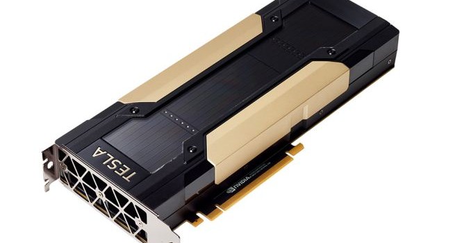
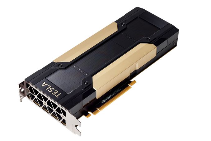
Similar to last year, at this year’s International Supercomputing Conference (ISC) NVIDIA has announced and detailed a PCI Express version of their latest Tesla GPU accelerator, the Volta-based V100. The conference itself runs from June 19 to 22, and with several speakers from NVIDIA scheduled for events tomorrow, NVIDIA is set to outline its next-generation efforts in HPC and deep learning with Volta.
With Volta discussed and described at their GPU Technology Conference in mid-May, NVIDIA upped the ante in terms of both features and reticle size: V100 is 815mm2 of custom TSMC 12FFN silicon, chock full of tensor cores and unified L1 cache per SM, along with many more fundamental – and as of yet not fully revealed – microarchitectural changes.
Like the previous Pascal iteration, the Tesla V100 PCIe offers a more traditional form factor as opposed to NVIDIA’s own mezzanine-type SXM2 form factor. This allows vendors to drop Tesla cards in traditional PCIe systems, making the cards far more accessible to server builders who don’t want to build around NVIDIA’s SXM2 connector or carrier board. The tradeoff being that the PCIe cards have a lower 250W TDP, and they don’t get NVLink, instead relying on just PCIe.
| NVIDIA Tesla Family Specification Comparison | ||||||
| Tesla V100 (SXM2) |
Tesla V100 (PCIe) |
Tesla P100 (SXM2) |
Tesla P100 (PCIe) |
|||
| CUDA Cores | 5120 | 5120 | 3584 | 3584 | ||
| Tensor Cores | 640 | 640 | N/A | N/A | ||
| Core Clock | ? | ? | 1328MHz | ? | ||
| Boost Clock(s) | 1455MHz | ~1370MHz | 1480MHz | 1300MHz | ||
| Memory Clock | 1.75Gbps HBM2 | 1.75Gbps HBM2 | 1.4Gbps HBM2 | 1.4Gbps HBM2 | ||
| Memory Bus Width | 4096-bit | 4096-bit | 4096-bit | 4096-bit | ||
| Memory Bandwidth | 900GB/sec | 900GB/sec | 720GB/sec | 720GB/sec | ||
| VRAM | 16GB | 16GB | 16GB | 16GB | ||
| L2 Cache | 6MB | 6MB | 4MB | 4MB | ||
| Half Precision | 30 TFLOPS | 28 TFLOPS | 21.2 TFLOPS | 18.7 TFLOPS | ||
| Single Precision | 15 TFLOPS | 14 TFLOPS | 10.6 TFLOPS | 9.3 TFLOPS | ||
| Double Precision | 7.5 TFLOPS (1/2 rate) |
7 TFLOPS (1/2 rate) |
5.3 TFLOPS (1/2 rate) |
4.7 TFLOPS (1/32 rate) |
||
| Tensor Performance (Deep Learning) |
120 TFLOPS | 112 TFLOPS | N/A | N/A | ||
| GPU | GV100 (815mm2) | GV100 (815mm2) | GP100 (610mm2) | GP100 (610mm2) | ||
| Transistor Count | 21B | 21B | 15.3B | 15.3B | ||
| TDP | 300W | 250W | 300W | 250W | ||
| Form Factor | Mezzanine (SXM2) | PCIe | Mezzanine (SXM2) | PCIe | ||
| Cooling | Passive | Passive | Passive | Passive | ||
| Manufacturing Process | TSMC 12nm FFN | TSMC 12nm FFN | TSMC 16nm FinFET | TSMC 16nm FinFET | ||
| Architecture | Volta | Volta | Pascal | Pascal | ||
On the surface, the addition of tensor cores is the most noticeable change. To recap, tensor cores can be liked to a series of unified ALUs that are able to multiply two 4×4 FP16 matrices together and subsequently add that product to an FP16 or FP32 4×4 matrix in a fused multiply add operation, as opposed to conventional FP32 or FP64 CUDA cores. In the end, this means that for very specific kinds (and specifically programmed) workloads, Volta can take advantage of the 100+ TFLOPS capability that NVIDIA has tossed into the mix.
As for the specific specifications of the PCIe Tesla V100, it’s similarly configured to the SXM2 version, getting the same number of CUDA cores and memory capacity, however operating at a lower clockspeed in-line with its reduced 250W TDP. Based on NVIDIA’s throughput figures, this puts the PCIe card’s boost clock at around 1370MHz, 85MHz (~6%) slower than the SXM2 version.
Interestingly, unlike the Tesla P100 family, NVIDIA isn’t offering a second-tier PCIe card based on salvaged chips; so this generation doesn’t have an equivalent to the 12GB PCIe Tesla P100. NVIDIA’s experience with GP100/interposer/HBM2 assembly as well as continuing production of HBM2 has likely reduced the need for memory-salvaged parts.
Finally, PCIe-based Tesla V100 accelerators are “expected to be available later this year from NVIDIA reseller partner and manufacturers,” including Hewlett Packard Enterprise, which will offer three different PCIe Volta systems.
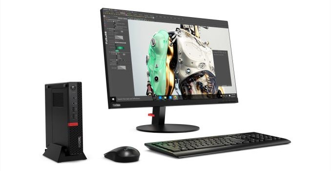
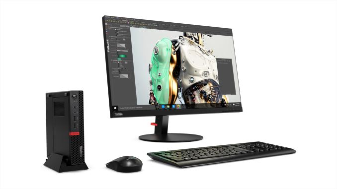
Lenovo has unveiled a new ThinkStation model, the P320 Tiny, based on a Kaby Lake / Q270 platform with NVIDIA’s Quadro P600 GPU. The unique aspect is the dimensions – At 1.4″ x 7.1″ x 7.2″ (1L in volume), it is one of the smallest systems we have see that includes a discrete GPU. In order to achieve this compact size, the 135W power adapter is external to the system.
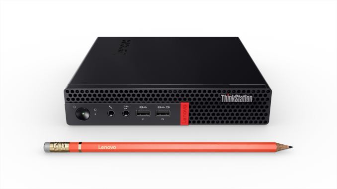
The P320 Tiny supports Kaby Lake CPUs with TDP of up to 35W (such as the Intel Core i7-7700T). NVIDIA’s Quadro P600 is a GP107-based GPU with a 40W TDP. The system comes with two DDR4 SODIMM slots and two M.2 NVMe SSD slots. There is a rich variety of I/O ports – audio jacks in the front, a total of six USB 3.0 ports spread across the front and the rear, a RJ-45 GbE port, and six display outputs (4x mini-DP + 2x DP). Thanks to the Quadro GPU, the P320 Tiny is able to come with ISV certifications for various applications such as AutoCAD etc.
| Lenovo ThinkStation P320 Tiny: General Specifications | |||
| CPU | Intel Kaby Lake (up to Core i7) (35W TDP max.) |
||
| Chipset | Intel Q270 | ||
| RAM | Up to 32 GB DDR4-2400 (2x SODIMM) | ||
| GPU | NVIDIA Quadro P600 | ||
| Storage | 2x M.2 PCIe: up to 1 TB NVMe SSD each ODD: optional with add-on |
||
| Networking | Gigabit Ethernet Intel 802.11 ac, 2 x 2, 2.4 GHz/5GHz + Bluetooth 4.0 – |
||
| I/O | 6x USB 3.0 Serial – optional |
||
| Dimensions | 1.4″ x 7.1″ x 7.2″ | ||
| Weight | 2.9 lbs | ||
The board used in the system seems to be a custom one – it is larger than a mini-STX board, but, smaller than an ITX one. It is perfect for space-constrained setups, and comes with extensibility options such as add-ons for extra USB ports and a COM port, or, for an optical drive, as shown in the gallery below.


As for operating systems, the new Lenovo ThinkStation P320 Tiny workstation supports both Windows and Linux. The P320 Tiny starts at $799 and is available now.
Building a PC is an experience worth having. Finding out what works with what and putting it all together is an experience, and the first time always gives a sense of achievement and accomplishment. In the high-end desktop space, even more so: trying …
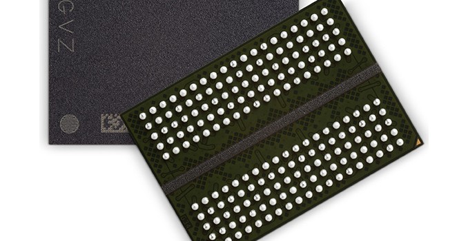

Micron has made a number of announcements in recent weeks regarding its GDDR memory for graphics cards, game consoles and networking applications. The company is reporting that they’ve been able to hit 16 Gbps data rates in the lab on their latest generation of GDDR5X devices, while also reiterating their long-term plans for GDDR6 and GDDR5, with GDDR6 memory due in a couple of quarters from now, while GDDR5 will be here to stay for a long time to come.
Graphics DRAM has been a hot topic in the industry in the recent years as GPU demands for memory bandwidth are growing rapidly and because different companies offer different types of memory to satisfy these increasing requirements. For example, SK Hynix and Samsung rolled out HBM (Gen 1 and Gen 2) memory in 2015 and 2016 for ultra-high-end consumer and HPC applications, whereas Micron introduced its GDDR5X for high-end graphics cards last year. At present, HBM offers the greatest potential bandwidth, however the complexity of the multi-layer chips and 2.5D packaging keep costs high, so it remains to be seen which mass consumer applications adopt it. Meanwhile, conventional graphics memory in BGA packaging and proven architecture continues to evolve and hit new performance targets due to architectural improvements, which are intended to keep it competitive in the coming years.
When Micron announced its GDDR5X memory in late 2015, it set two targets for data transfer rates: the initial target of 10 – 12 Gbps and the longer-term target of 16 Gbps. Initially, the company only supplied GDDR5X ICs validated at 10 and 11 Gbps, but this year the company also started to bin the chips for 12 Gbps. The latter are used on NVIDIA’s Titan Xp graphics card. What is noteworthy is that engineers from Micron’s development center in Munich (also known as Graphics DRAM Design Center) recently managed to run the company’s mass-produced GDDR5X chips at 16 Gbps in the lab.
While the achievement doesn’t have an impact on actual products available today, it has a number of important implications. Primarily, it means that Micron has refined their process to the point where they can build graphics DRAM with 16 Gbps signaling, and this is something it is going to need going forward. But additionally, it shows that the current GDDR5X technology has potential, and that Micron’s customers might release new products with faster memory.
Micron has been quite busy in the last couple of years working on the GDDR5X memory specification, physical implementation of such ICs, and then developing GDDR6 chips that the company plans to launch by early 2018. In fact, GDDR5X and the GDDR6 are not that different. They are both based on the 16n prefetch architecture and this is the key to their additional performance when compared to GDDR5. Meanwhile, GDDR6 also features dual-channel mode, which is meant to ensure better channel utilization and hence improve performance in cases that can take advantage of the feature.
| Micron’s GDDR Memory at Glance | |||||
| GDDR5 | GDDR5X | GDDR6 | |||
| Capacity | 4 Gb – 8 Gb | 8 Gb | 8 Gb | ||
| Data Rate | 5 – 8 Gbps | 10 – 12 Gbps | Over 12 Gbps | ||
| Process Technology | 20+ nm 20 nm, 16 nm |
20 nm | 16 nm | ||
Meanwhile Micron will be using 16 nm fab lines to produce GDDR6 memory devices, which may add frequency potential to the upcoming chips compared to ICs made using their 20 nm fabrication process. Speaking of 16 nm, Micron also plans to use it for newer GDDR5 chips, which makes a lot of sense considering the fact that such devices are going to be used for graphics cards and game consoles for years to come.
Summing up. Micron has GDDR5X memory chips that run at 16 Gbps in the lab using test equipment. Such chips are made using 20 nm process technology. Meanwhile Micron is using 16 nm fabrication process to produce GDDR6 and GDDR5 by 2018.
Related Reading: