News


ZOTAC Announces VR GO Backpack PC with GeForce GTX 1070

ZOTAC Announces VR GO Backpack PC with GeForce GTX 1070

ZOTAC this week has formally introduced its VR GO backpack PC designed for virtual reality enthusiasts. The system is equipped with NVIDIA’s GeForce GTX 1070 graphics, a quad-core CPU from Intel, rich I/O capabilities and a hot-swappable battery. Despite its positioning, the VR GO can be used like a normal desktop computer, which differentiates it from early prototypes of wearable VR PCs from other makers.

ZOTAC is mostly known for its graphics cards and high-performance small form-factor PCs, but not wearable systems (which are not that uncommon: industrial- and even space-grade wearable PCs have existed for years). To develop its VR GO computer, the company had to use experience it obtained from building SFF systems for gamers as well as to find ways to minimize weight and to ensure that the design can handle harsh treatment during gaming sessions. Basically, ZOTAC had to fix everything tightly inside the box while ensuring appropriate cooling and proper position of the I/O ports.

To make it convenient to connect a VR headset to the VR GO, one side of the device has the appropriate ports. The single side has one HDMI output, two USB 3.0 ports and one power connector on top of it. Such positioning greatly simplifies cable management and makes VR gaming with a PC on your back a little more comfortable. The system also comes with a removable battery pack that enables autonomous operation for (waiting on offical numbers) hours.

While virtual reality is considered as an important milestone for gaming, it hardly makes sense to develop a PC only for VR, which is why ZOTAC’s VR GO is a powerful PC in general and can be used like a desktop computer too. It has three additional USB 3.0/3.1 Type-A connectors, an SD card reader, four additional display outputs (two HDMI, two DP), two GbE ports as well as two 3.5 mm audio jacks.

Inside the ZOTAC VR GO there is a custom motherboard in a proprietary form-factor carrying an Intel Core i7 CPU, two DDR4 SO-DIMMs, an M.2 SSD (PCIe 3.0 x4), an 802.11ac Wi-Fi module and NVIDIA’s GeForce GTX 1070 MXM module. To cool down the CPU and the GPU (a total TDP of 150 W), ZOTAC uses a proprietary low-profile air cooling system but has not disclosed details. At this point, we do not know whether the manufacturer reinforced the design of its cooler’s backplate somehow, but this is a logical thing to expect. To expand the storage capacity of the system, ZOTAC also added one bay for a SATA-based 2.5″ storage device (either HDD, which might be affected by rapid movement, or a high capacity TLC SSD).

ZOTAC’s VR GO system is not the first backpack-type PC developed by the company. At Computex 2016 the hardware manufacturer already demonstrated a wearable system, but that was largely a prototype and still in the early design stage. By contrast, the VR GO looks like a commercial product.

ZOTAC does not specify exact availability timeframe for its VR GO backpack PC other than Q4 2016 as well as its estimated price. We expect to see it at CES in early January for sure.

Related Reading


ZOTAC Announces VR GO Backpack PC with GeForce GTX 1070

ZOTAC Announces VR GO Backpack PC with GeForce GTX 1070

ZOTAC this week has formally introduced its VR GO backpack PC designed for virtual reality enthusiasts. The system is equipped with NVIDIA’s GeForce GTX 1070 graphics, a quad-core CPU from Intel, rich I/O capabilities and a hot-swappable battery. Despite its positioning, the VR GO can be used like a normal desktop computer, which differentiates it from early prototypes of wearable VR PCs from other makers.

ZOTAC is mostly known for its graphics cards and high-performance small form-factor PCs, but not wearable systems (which are not that uncommon: industrial- and even space-grade wearable PCs have existed for years). To develop its VR GO computer, the company had to use experience it obtained from building SFF systems for gamers as well as to find ways to minimize weight and to ensure that the design can handle harsh treatment during gaming sessions. Basically, ZOTAC had to fix everything tightly inside the box while ensuring appropriate cooling and proper position of the I/O ports.

To make it convenient to connect a VR headset to the VR GO, one side of the device has the appropriate ports. The single side has one HDMI output, two USB 3.0 ports and one power connector on top of it. Such positioning greatly simplifies cable management and makes VR gaming with a PC on your back a little more comfortable. The system also comes with a removable battery pack that enables autonomous operation for (waiting on offical numbers) hours.

While virtual reality is considered as an important milestone for gaming, it hardly makes sense to develop a PC only for VR, which is why ZOTAC’s VR GO is a powerful PC in general and can be used like a desktop computer too. It has three additional USB 3.0/3.1 Type-A connectors, an SD card reader, four additional display outputs (two HDMI, two DP), two GbE ports as well as two 3.5 mm audio jacks.

Inside the ZOTAC VR GO there is a custom motherboard in a proprietary form-factor carrying an Intel Core i7 CPU, two DDR4 SO-DIMMs, an M.2 SSD (PCIe 3.0 x4), an 802.11ac Wi-Fi module and NVIDIA’s GeForce GTX 1070 MXM module. To cool down the CPU and the GPU (a total TDP of 150 W), ZOTAC uses a proprietary low-profile air cooling system but has not disclosed details. At this point, we do not know whether the manufacturer reinforced the design of its cooler’s backplate somehow, but this is a logical thing to expect. To expand the storage capacity of the system, ZOTAC also added one bay for a SATA-based 2.5″ storage device (either HDD, which might be affected by rapid movement, or a high capacity TLC SSD).

ZOTAC’s VR GO system is not the first backpack-type PC developed by the company. At Computex 2016 the hardware manufacturer already demonstrated a wearable system, but that was largely a prototype and still in the early design stage. By contrast, the VR GO looks like a commercial product.

ZOTAC does not specify exact availability timeframe for its VR GO backpack PC other than Q4 2016 as well as its estimated price. We expect to see it at CES in early January for sure.

Related Reading


LaCie Announces Bolt3: 2 TB External SSD at 2.8 GBps over Thunderbolt 3

LaCie Announces Bolt3: 2 TB External SSD at 2.8 GBps over Thunderbolt 3

LaCie this week has introduced its first external solid-state storage solution using Thunderbolt. The Bolt3 uses two M.2 SSDs in RAID 0 mode to enable 2 TB of storage as well as up to 2800 MB/s data rate, which is the highest level of performance offered by an available commercial DAS device. The Bolt3 is being advertised for video professionals who edit 4K (and up) video.

The LaCie Bolt3 (STFF2000400) packs in two 1 TB NVMe SSDs in M.2 form-factor that work in RAID 0 mode to enable up to 2800 MB/s read and up to 2200 MB/s write speeds. Seagate, the owner of the LaCie brand, does not disclose which SSDs the device has under the hood, but the company states that the Bolt3 was designed with long-term reliability in mind. This might imply that the device uses drives with high endurance (although, we cannot say whether the maker uses datacenter-grade SSDs). The external storage solution can realize its whole potential when connected to a TB3-enabled computer using the active Thunderbolt 3 cable that is bundled with the device. The Bolt3 also has another TB3 receptacle so to daisy chain more Thunderbolt 3 devices (storage or display) or even charge them (the Bolt3 has its own external PSU).

LaCie Bolt3 Specifications
  STFF2000400
SSD Model 2 × SSDs
Controller unknown
NAND Flash MLC NAND
Form-Factor, Interface M.2-2280, PCIe 3.0 x4, NVMe 1.2
Sequential Read 2800 MB/s
Sequential Write 2200 MB/s
Random Read IOPS unknown
Random Write IOPS unknown
Pseudo-SLC Caching unknown
DRAM Buffer unknown
Security Software-based AES-256 encryption
Warranty 2 years
MSRP $1999

From an aesthetic point of view, the LaCie Bolt3 is designed to be seen on a desk. It is made of black aluminum, it features a blue LED on the backside and the enclosure is tilted by 45° to its stand. The mounting mechanism uses neodymium magnets that firmly attach the Bolt3 to its stand, but allow to quickly detach it and transport anywhere. Users can have the drive flat as well. To ensure long-term reliability of SSDs inside, the Bolt3 also has active cooling.

The LaCie Bolt3 belongs to the company’s limited edition series which are designed to promote performance as well as eye-catching design. This means it doesn’t come cheap. The LaCie Bolt3 2 TB will be available this quarter for $1999, which is well beyond the price of consumer SSD storage and more than one would have to pay for a DIY 2 TB Thunderbolt 3 external storage solution. As the LaCie Bolt3 is the fastest off-the-shelf external storage solution available today, the manufacturer wants to charge a premium.

LaCie Announces Bolt3: 2 TB External SSD at 2.8 GBps over Thunderbolt 3

LaCie Announces Bolt3: 2 TB External SSD at 2.8 GBps over Thunderbolt 3

LaCie this week has introduced its first external solid-state storage solution using Thunderbolt. The Bolt3 uses two M.2 SSDs in RAID 0 mode to enable 2 TB of storage as well as up to 2800 MB/s data rate, which is the highest level of performance offered by an available commercial DAS device. The Bolt3 is being advertised for video professionals who edit 4K (and up) video.

The LaCie Bolt3 (STFF2000400) packs in two 1 TB NVMe SSDs in M.2 form-factor that work in RAID 0 mode to enable up to 2800 MB/s read and up to 2200 MB/s write speeds. Seagate, the owner of the LaCie brand, does not disclose which SSDs the device has under the hood, but the company states that the Bolt3 was designed with long-term reliability in mind. This might imply that the device uses drives with high endurance (although, we cannot say whether the maker uses datacenter-grade SSDs). The external storage solution can realize its whole potential when connected to a TB3-enabled computer using the active Thunderbolt 3 cable that is bundled with the device. The Bolt3 also has another TB3 receptacle so to daisy chain more Thunderbolt 3 devices (storage or display) or even charge them (the Bolt3 has its own external PSU).

LaCie Bolt3 Specifications
  STFF2000400
SSD Model 2 × SSDs
Controller unknown
NAND Flash MLC NAND
Form-Factor, Interface M.2-2280, PCIe 3.0 x4, NVMe 1.2
Sequential Read 2800 MB/s
Sequential Write 2200 MB/s
Random Read IOPS unknown
Random Write IOPS unknown
Pseudo-SLC Caching unknown
DRAM Buffer unknown
Security Software-based AES-256 encryption
Warranty 2 years
MSRP $1999

From an aesthetic point of view, the LaCie Bolt3 is designed to be seen on a desk. It is made of black aluminum, it features a blue LED on the backside and the enclosure is tilted by 45° to its stand. The mounting mechanism uses neodymium magnets that firmly attach the Bolt3 to its stand, but allow to quickly detach it and transport anywhere. Users can have the drive flat as well. To ensure long-term reliability of SSDs inside, the Bolt3 also has active cooling.

The LaCie Bolt3 belongs to the company’s limited edition series which are designed to promote performance as well as eye-catching design. This means it doesn’t come cheap. The LaCie Bolt3 2 TB will be available this quarter for $1999, which is well beyond the price of consumer SSD storage and more than one would have to pay for a DIY 2 TB Thunderbolt 3 external storage solution. As the LaCie Bolt3 is the fastest off-the-shelf external storage solution available today, the manufacturer wants to charge a premium.

Microsoft Lifts the Lid on Some Intel Skylake-EP Details via the Open Compute Project

Microsoft Lifts the Lid on Some Intel Skylake-EP Details via the Open Compute Project

As part of the European Digital Infrastructure Summit in London this week, Microsoft’s Azure team will be lifting the lid on Project Olympus, the next generation hyperscale cloud hardware design and model for open source hardware development, in collaboration with the Open Compute Project (OCP). Project Olympus is being described as a way to embrace future platforms in a standardized design, much like other OCP projects, and the open source standards behind the platform are offering insights into Intel’s Skylake-EP Platform, known as Purley.

It seems odd for information about Skylake-EP to be sanctioned at this time (technically none of the documents mention Intel, Skylake or Purley, but it can be deciphered as below), especially given the recent release of Broadwell-E/EP and Intel’s previous stance of limited data release prior to launch. It would appear that the information Microsoft are providing at the summit has been sanctioned, however sometimes putting two plus two together requires a little digging.

All this information is posted on the Microsoft Azure blog, which links directly to the OCP pages where motherboard specifications and server mechanical specifications are provided in PDF format.

It’s a Socket We’ve Seen Before, Which Can Make Waves

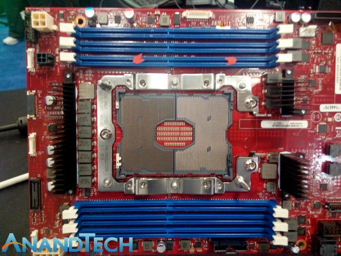
Being the motherboard guy at AnandTech, I skipped straight to the motherboard information. Page 31 of the motherboard document gives the following example motherboard drawing:

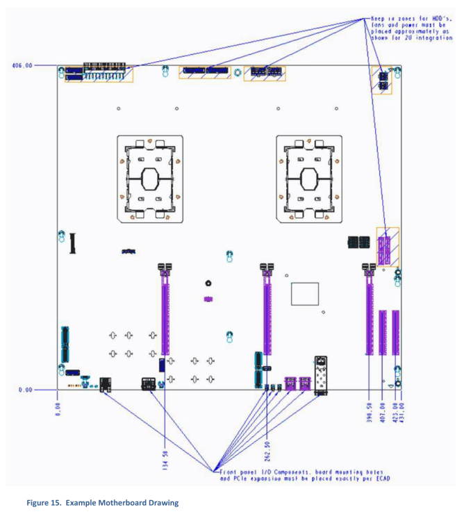
Here is a dual-socket design, with a set of PCIe slots, some power connectors and other I/O components (some fiber Ethernet, for example). But jam packed in the middle are two very large sockets. We’ve seen these before, back at Supercomputing 2015 when Intel announced Knights Landing, which is a Xeon Phi product:

Xeon Phi’s Knights Landing design uses an LGA3647 implementation based on its 72 cores, 16GB of MCDRAM, and six memory channels. There are a lot of pins because there’s a lot to power up.

In previous generations of EP processors, both EP and E have shared the same socket. If I wanted to use my E5-2699 v4 Broadwell-EP LGA2011-3 processor in an X99 consumer motherboard instead of an i7-6950X, I could. Essentially all the Core and all the Xeon E5 CPUs have shared a common socket, making it easy for 1P/2P/4P processors to share around.  If Purley / Skylake-EP uses the LGA3647 socket, this means one of four things.

The first is that this might not be Skylake-EP, and something odd like Skylake-EN.

The second is that Skylake-E will also share the same socket, and be LGA3647. This sounds somewhat implausible, given that Skylake-EP will have to handle at least the same amount of cores as Broadwell-EP, so there would be a lot of pins on a consumer platform for no reason.

The third possibility is that Skylake-E and Skylake-EP are going to be different sockets. This would indicate a split between consumer HEDT and dual-socket workstations and servers. Given previous generational changes, Skylake-E for consumers is expected to follow a similar pattern – around 2000 pins in a single socket design. However if Skylake-EP is making the jump to a significantly larger socket, especially for 2P workstation and server designs, it will produce a spread of difference in potential for pricing structures and implementation.

The fourth possibility extends from the third, and that Skylake-EP will have two socket designs depending on the size of the core. For Broadwell-EP, there were three designs for the silicon underneath – a low core count (LCC), a medium core count (MCC) and an extreme core count (XCC). If Intel are splitting up the sockets, it may be the case that only the XCC or MCC+XCC sides of the equation are using LGA3647. LCC designs are typically used for the consumer E series parts anyway, so Intel may decide to make the low core designs of EP on the smaller socket. There’s a wealth of possibility here.

I Heard You Like RAM. I Heard You Like Storage.

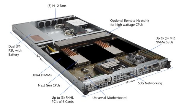
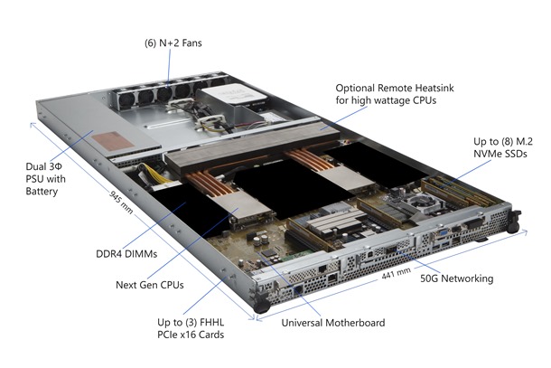
On the main Microsoft Azure page, a handy diagram of an example machine was provided (with some areas blacked out):

Here we see that motherboard from the image above, using two low profile heatsinks with copper piping feeding an optional heatsink inside the chassis. To the sides of each of the sockets are big black squares, indicating where the DDR4 memory should go. Nearer the bottom of the board are networking implementations (50G is labeled), and PCIe slots suitable for three full-height, half-length (FHHL) PCIe cards.  Interestingly on the right-hand side, we have labeled ‘up to 8 M.2 NVMe SSDs’.

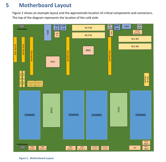
Back to the motherboard specification, we see the list of blacked out areas along with a more comprehensive sequence of potential configurations:

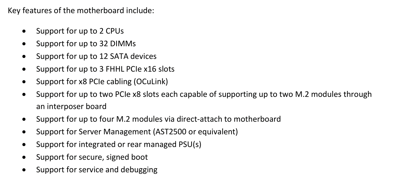
There are spots for up to 32 DIMMs, which makes 16 per socket. Depending on how many memory controllers the CPU has, this could mean 8-channel and 2 DIMMs per channel (DPC), or 4-channel and 4 DPC. Nowhere does it state the maximum DRAM support per CPU, but DDR4 LRDIMMs are currently at 256GB/module, meaning a potential maximum of 4TB per CPU or 8TB per system. We expect Skylake-EP to support 3D XPoint at some stage as well.

On that list of support also mentions up to 12 SATA devices, up to 3 FHHL cards, and two PCIe x8 slots capable of supporting two M.2 modules each. So this is where that 8x M.2 comes in – if we get four from two PCIe x8 slots, and combine this with up to four M.2 direct attach modules, that makes eight.

The top-level block diagram is also worth a look. Patrick from STH specifically points out the PCIe 3.0 support for the platform:

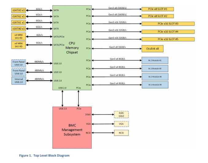
On the right-hand side, adding up all the PCIe numbers and it comes to 88 PCIe 3.0 lanes, or 44 per CPU. This would be an upgrade on the 40 lanes per CPU currently on Broadwell-EP. There is also provision for PCIe lanes to be used with the mini-SAS connectors on the left-hand side. Technically the BMC also requires a PCIe link as well.

So When?

Given the long product cycles of Intel’s EP platforms, and the fact that the Big Seven cloud providers have a lot of clout over sales means they are most likely testing and integrating the next generation hardware. The release to the public, and smaller players in the OCP space, is a long and slow one. We’re not expecting Skylake-E/EP out until well into 2017, if not the year after, so information will certainly be on the slow burn. Supercomputing 2016 is happening in Utah in a couple of weeks, and although we won’t be there due to scheduling, something may pop out of the woodwork. We’ll keep our eyes peeled.

Source: Microsoft, ServeTheHome

Related Reading

SuperComputing 15: Intel’s Knights Landing / Xeon Phi Silicon on Display
A Few Notes on Intel’s Knights Landing and MCDRAM Modes from SC15
The Next Generation Open Compute Hardware: Tried and Tested
The Intel Xeon E5 v4 Review: Testing Broadwell-EP With Demanding Server Workloads