Semiconductors


TSMC Kicks Off Volume Production of 7nm Chips

TSMC Kicks Off Volume Production of 7nm Chips

TSMC last week announced that it had started high volume production (HVM) of chips using their first-gen 7 nm (CLN7FF) process technology. The contract maker of semiconductors says it has over a dozen of customers with tens of designs eager to use the…

TSMC Starts to Build Fab 18: 5 nm, Volume Production in Early 2020

TSMC Starts to Build Fab 18: 5 nm, Volume Production in Early 2020

TSMC last week held a groundbreaking ceremony for its Fab 18 phase 1 production facility. The fab will produce chips using TSMC’s 5 nm process starting from early 2020. When all three phases of the manufacturing facility are completed, its wafer starts capacity will exceed one million 300-mm wafers per year, comparable with other three GigaFabs operated by TSMC.

TSMC’s Fab 18 will be located in Tainan (in the Southern Taiwan Science Park), and will be built in three phases. The construction of the first phase or segment of the building will be completed in about a year from now, after which TSMC will move in equipment sometime in early 2019. In about two years from now, the company expects to start volume production of chips using its 5 nm process technology at the Fab 18/phase 1. Construction of the second and the third phases will commence in Q3 2018 and Q3 2019. The two phases will start volume production in 2020 and 2021, respectively.

TSMC’s Fab 18: Milestones
  Phase 1 Phase 2 Phase 3
Construction Start Early 2018 Q3 2018 Q3 2019
Equipment Move-In Early 2019 ? ?
High-Volume Manufacturing Start Early 2020 2020 2021

The Fab 18 will have a total floor area of 950,000 square meters and its cleanroom area will exceed 160,000 square meters, the contract maker of semiconductors said. TSMC estimates that the combined production capacity of all three phases of the Fab 18 will exceed one million 300-mm wafer starts per year, which is comparable to the capacities of the other GigaFabs that TSMC operates — Fab 12, Fab 14, and Fab 15. It is noteworthy that the planned floor area and cleanroom space of the Fab 18 will be significantly larger than the initially planned floor and cleanroom area of the Fab 15, which emphasizes increasing complexity of IC manufacturing these days as well as increasing orders from TSMC’s clients.  In total, the Fab 18 will cost TSMC NT$500 billion ($17.08 billion), making it one of the most expensive chip manufacturing facilities in the world.

Brief Comparison of TSMC’s Fab 15 and Fab 18
  Fab 15 Fab 18
Total Area of Site 18.4 hectares ?
Building Area 430,000 m² 950,000 m²
Clean Room Space* 104,000 m² 160,000 m²
Initially Expected Investment** NT$300 billion
~$9.375 billion
NT$500 billion
~$17.08 billion
Groundbreaking July 2010 January 2018
Notes *Fabs are usually upgraded over time, today’s cleanroom space of the Fab 15 may be larger than initially projected.
**Initially expected investments tend to change over time.

Besides its dimensions and cost, there is another reason why Fab 18 is important for the semiconductor industry: it will be one of the world’s first facilities to produce chips using a 5-nm production tech. TSMC yet has to detail its 5 nm manufacturing technology, but from the announcements that the company has made so far it is evident that this fabrication process will rely significantly on EUV lithography. TSMC did not mention EUV at all in its press release, which is a bit strange. Meanwhile, over the course of last year the semiconductor manufacturer did mention that the 5 nm fabrication technology would be its second-gen EUV process, which means usage of EUV for more more layers when compared to the CLN7FF+ (its advanced 7 nm tech). Furthermore, TSMC already has functional SRAM cells made using its CLN5FF technology and the yields were satisfactory in mid-2017. Therefore, the 5 nm development process seems to be going on relatively well.

The extended usage of EUV for 5-nm chip production means that the company will need to install more EUV tools into the Fab 18, which is one of the reasons why it needed to expand the fab’s cleanroom space. The fact that TSMC has begun to build Fab 18 indicates that the contract maker of chips is confident in its 5 nm technology as well as EUV equipment, including ASML’s TWINSCAN NXE scanners, Cymer’s EUV light sources and other tools. This confidence is further underscored by their intention to start high-volume manufacturing of 5-nm devices in Fab 18 in early 2020.

Advertised PPA Improvements of TSMC’s CLN7FF Nodes
Data announced by TSMC during conference calls, press briefings and in press releases
  7FF
vs
16FF+
7FF
vs
10FF
7FF EUV
vs
7FF
5FF EUV
vs
7FF EUV
Power 60% <40% 10% lower
Performance 30% ? lower higher
Area Reduction 70% >37% ~10% tangible
HVM Start ~Q2 2018 ~H2 2019 H1 2020

Related Reading:

Sources: TSMC (1, 2, 3, 4)

GlobalFoundries Details 7 nm Plans: Three Generations, 700 mm², HVM in 2018

GlobalFoundries Details 7 nm Plans: Three Generations, 700 mm², HVM in 2018

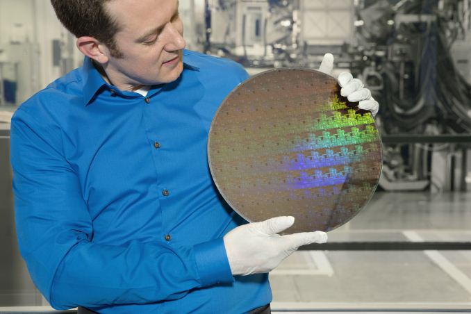
Keeping an eye on the ever-evolving world of silicon lithography, GlobalFoundries has recently disclosed additional details about its 7 nm generation of process technologies. As announced last September, the company is going to have multiple generations of 7 nm FinFET fabrication processes, including those using EUV. GlobalFoundries now tells us that its 7LP (7 nm leading performance) technology will extend to three generations and will enable its customers to build chips that are up to 700 mm² in size. Manufacturing of the first chips using their 7LP fabrication process will ramp up in the second half of 2018.

GlobalFoundries 7LP Platform
  7nm Gen 1 7nm Gen 2 7nm Gen 3
Lithography DUV DUV + EUV DUV + EUV
Key Features Increased performance, lower power, higher transistor density vs. 14LPP. Increased yields and lower cycle times. Performance, power and area refinements.
Reasons for EUV insertion To reduce usage of quadruple and triple patterning. To improve line-edge roughness, resolution, CD uniformity, etc.
HVM Start 2H 2018 2019 (?) 2020 (?)

7 nm DUV

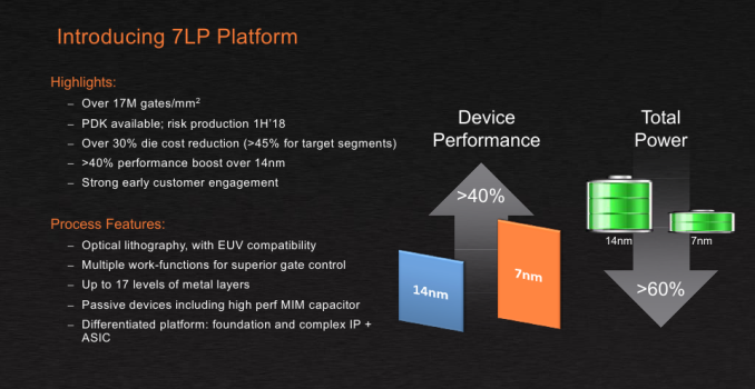
First and foremost, GlobalFoundries reiterated their specs of their first-gen 7 nm process, which involves deep ultraviolet (DUV) lithography with argon fluoride (ArF) excimer lasers operating on a 193 nm wavelength. The company’s 7 nm fabrication process is projected to bring over a 40% frequency potential over the 14LPP manufacturing technology that GlobalFoundries uses today, assuming the same transistor count and power. The tech will also reduce the power consumption of ICs by 60% at the same frequency and complexity.

For their newest node, the company is focusing on two ways to reduce power consumption of the chips: implementing superior gate control, and reducing voltages. To that end, chips made using GlobalFoundries’ 7LP technology will support 0.65 – 1 V, which is lower than ICs produced using the company’s 14LPP fabrication process today. In addition, 7LP semiconductors will feature numerous work-functions for gate control.

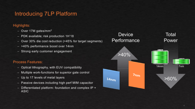
When it comes to costs and scaling, the gains from 7LP are expected to be a bit atypical from the usual manufacturing process node advancement. On the one hand, the 7 nm DUV will enable over 50% scaling over 14LPP, which is not something surprising given the fact that the latter uses 20 nm BEOL interconnections. However, since 7 nm DUV involves more layers that require triple and quadruple patterning, according to the foundry the actual die cost reduction will be in the range between 30% and 45% depending on application.

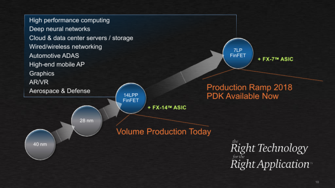
The 7 nm platform of GlobalFoundries is called 7LP for a reason — the company is targeting primarily high-performance applications, not just SoCs for smartphones, which contrasts to TSMC’s approach to 7 nm. GlobalFoundries intends to produce a variety of chips using the tech, including CPUs for high-performance computing, GPUs, mobile SoCs, chips for aerospace and defense, as well as automotive applications. That said, in addition to improved transistor density (up to 17 million gates per mm2 for mainstream designs) and frequency potential, GlobalFoundries also expects to increase the maximum die size of 7LP chips to approximately 700 mm², up from the roughly 650 mm² limit for ICs the company is producing today. In fact, when it comes to the maximum die sizes of chips, there are certain tools-related limitations.

Advertised PPA Improvements of New Process Technologies
Data announced by companies during conference calls, press briefings and in press releases
  GlobalFoundries
7nm Gen 1
vs 14LPP
7nm Gen 2
vs Gen 1
7nm Gen 3
vs Gen 1/2
Power >60% same* lower
Performance >40% same* higher
Area Reduction >50% none yes
*Better yields could enable fabless designers of semiconductors to bin chips for extra performance or lower power.

GlobalFoundries has been processing test wafers using 7 nm process technology for clients for several quarters now. The company’s customers are already working on chips that will be made using 7 nm DUV process technology, and the company intends to start risk production of such ICs early in 2018. Right now, the clients are using the 0.5 version of GlobalFoundries’ 7 nm process design kit (PDK), and later this year the foundry will release PDK v. 0.9, which will be nearly final version of the kit. Keep in mind that large customers of GlobalFoundries (such as AMD) do not need the final version of the PDK to start development of their CPUs or GPUs for a given node, hence, when GF talks about plans to commercialize its 7LP manufacturing process, it means primarily early adopters — large fabless suppliers of semiconductors.

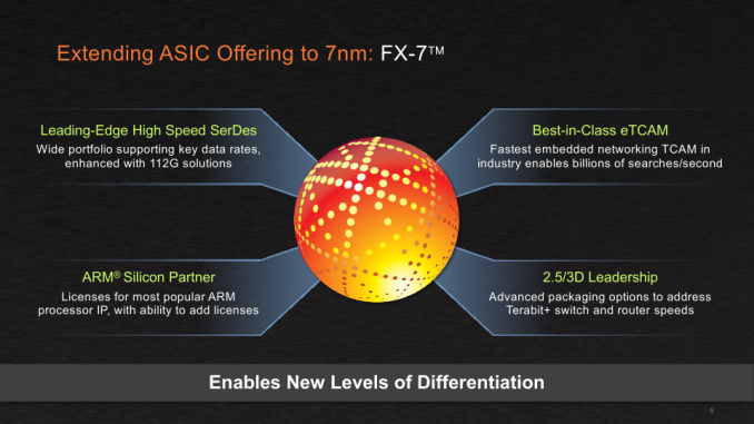
In addition to its PDKs, GlobalFoundries has a wide portfolio of licenses for ARM CPU IP, high-speed SerDes (including 112G), and 2.5D/3D packaging options for its 7LP platform. When it comes to large customers, GlobalFoundries is ready for commercial production of chips using its 7 nm DUV fabrication process in 2018.

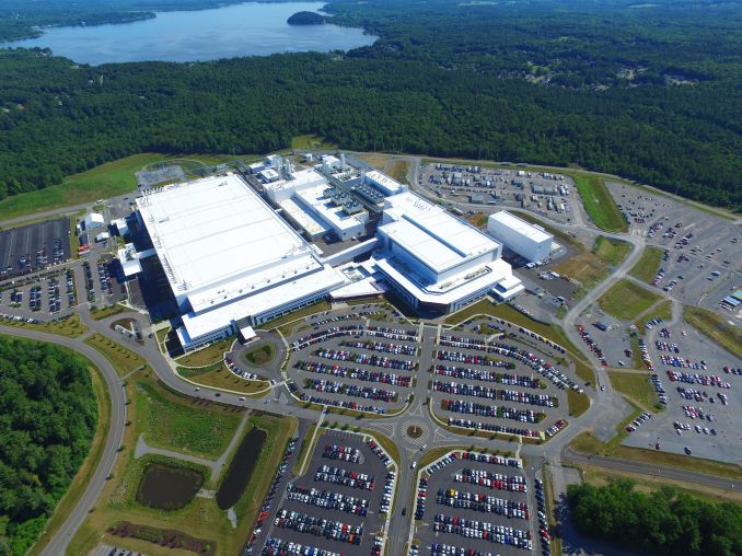
Fab 8 Ready for 7LP, Getting Ready for EUV

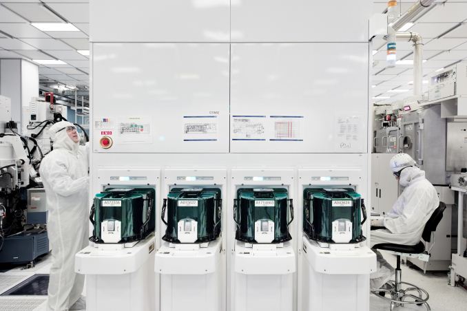
Speaking of high volume manufacturing using their 7LP DUV process, it is necessary to note that earlier this year GlobalFoundries announced plans to increase the production capacity of their Fab 8. Right now, the output of Fab 8 is around 60,000 wafer starts per month (WSPM), and the company expects to increase it by 20% for 14LPP process technology after the enhancements are complete.

The expansion does not involve physical enhancement of the building, which may indicate that the company intends to install more advanced scanners with increased output capabilities. GlobalFoundries naturally does not disclose details about the equipment it uses, but newer scanners with higher output and better overlay and focus performance will also play their role in HVM using 7 nm DUV that relies on quadruple patterning for select layers.

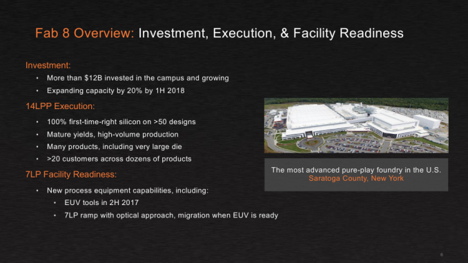
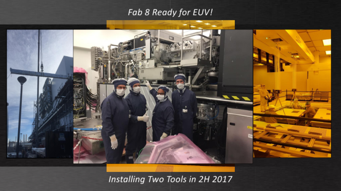
In addition to more advanced ASML TWINSCAN NXT DUV equipment, GlobalFoundries plans to install two TWNSCAN NXE EUV scanners into the Fab 8 in the second half of this year. This is actually a big deal because current-generation fabs were not built with EUV tools in mind. Meanwhile, EUV equipment takes up more space than DUV equipment because of the light source and other aspects.

EUV: Many Problems Solved, But Concerns Remain

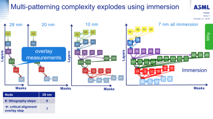
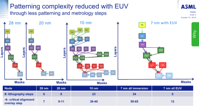
Usage of multi patterning for ultra-thin process technologies is one of the reason why the industry needs lithography that uses extreme ultraviolet wavelength of 13.5 nm. As avid readers know, the industry has been struggling to develop EUV tools suitable for HVM, and while significant progress has been made recently, EUV is still not quite up to scale. This is exactly why GlobalFoundries is taking a cautious approach to EUV that involves multiple generations. Keep in mind that GlobalFoundries does not seem to have official names for different iterations of its 7 nm process technologies. The only thing that the company is talking about now is its “7LP platform with EUV compatibility.” Therefore, all our generations-related musings here are just for a better understanding of what to expect.

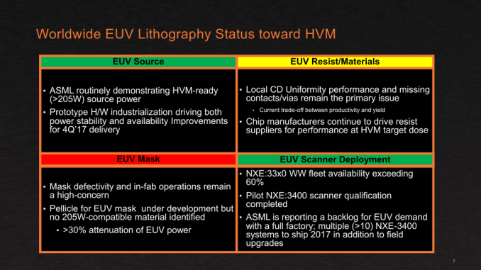
ASML has developed several generations of EUV scanners and has demonstrated light sources with 205 W of power. The latest TWINSCAN NXE scanners with recent upgrades have demonstrated an availability that exceeds 60%, which is good enough to start their deployment, according to GlobalFoundries. Eventually, availability is expected to increase to 90%, in line with DUV tools.

Meanwhile, there are still concerns about protective pellicles (films) for EUV photomasks, mask defects, as well as EUV resists. On the one hand, current pellicles can handle productivity rates of up to 85 wafers per hour (WpH), which is well below 125 WpH planned for this year. Basically, this means that existing pellicles cannot handle powerful light sources required for HVM. Any defect on a pellicle can affect wafers and dramatically lower yields. Intel demonstrated pelliclized photomasks that could sustain over 200 wafer exposures, but we do not know when such pellicles are expected to enter mass production. On the other hand, powerful light sources are required for satisfactory line-edge roughness (LER) and local critical dimensions (CD) uniformity primarily because of imperfections of resists.

7 nm EUV Gen 1: Improving Yields, Reducing Cycles

Given all the EUV-related concerns, GlobalFoundries will start to insert EUV for select layers in a bid to reduce the usage of multi patterning (and eliminate quadruple patterning in general, if possible), thereby improving yields. At this time the company is not disclosing when it plans to start using EUV tools for manufacturing, only stating that they’ll do so “when it is ready.” It is unlikely that EUV will be ready in 2018, so it is logical to expect the company to use EUV tools no sooner than 2019.

Such approach makes a lot of sense because it enables GlobalFoundries to increase yields for its customers and to learn more about what it will take to get EUV ready for HVM. In the best-case scenario, GlobalFoundries will be able to produce designs developed for 7 nm DUV with multi patterning using its 7 nm EUV tech. However, one should keep in mind two factors. First, semiconductor developers release new products every year. Second, GlobalFoundries will begin to insert EUV tools into production at least a couple of quarters after the launch of the first 7 nm DUV chips. Therefore, it is highly likely that the first EUV-based chips produced at GlobalFoundries will be new designs rather than chips originally fabbed on the all-DUV process.

7 nm EUV Gen 2: Higher Transistor Density and Line-Edge Roughness

Depending how fast the industry addresses the current EUV challenges related to masks, pellicles, CD uniformity, LER and other things, GlobalFoundries will eventually roll out another generation of its 7 nm EUV process.

The second-gen 7 nm EUV manufacturing technology from GlobalFoundries will feature improved LER and a better resolution, which the company hopes will enable higher transistor densities with lower power and/or higher performance. Though given the experimental nature of the tech behind this process, as you’d expect GlobalFoundries is not saying when certain problems are to be resolved and when it can offer appropriate services to its customers.

Finally, 3rd Gen 7LP will likely introduce some new design rules to enable geometry scaling and/or higher frequencies/lower power, but in general I’m expecting that the transition to this process should be relatively seamless to IC designers. After all, the majority of layers will still use DUV. The only question is whether GlobalFoundries will need to install additional TWINSCAN NXE scanners into the Fab 8 for its 2nd Gen 7 nm EUV process technologies, which would also indicate that the number of layers processed using EUV had increased.

5 nm EUV: Adjustable Gate-All-Around FETs

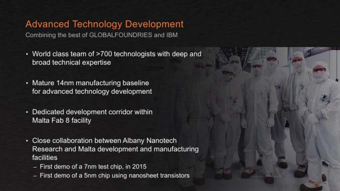
A week before GlobalFoundries disclosed their 7LP platform plans, IBM and their Research Alliance partners (GlobalFoundries and Samsung) demonstrated a wafer processed using a 5 nm manufacturing process. ICs on the wafer were built using silicon nanosheet transistors (aka gate-all-around FETs [GAA FETs]) and it looks like they will be building blocks for semiconductors in the future. The big question of course is when.

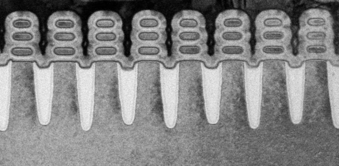
GAA FETs developed by IBM, GlobalFoundries, and Samsung stack silicon nanosheets in such a way that every transistor now has four gates. The key thing about GAA FETs is that the width of nanosheets can be adjusted within a single manufacturing process or even within the IC design to fine-tune performance or power consumption. When it comes to performance/power/area(PPA)-related improvements, IBM claims that when compared to a 10 nm manufacturing process, the 5 nm technology offers 40% performance improvement at the same power and complexity, or 75% power savings at the same frequency and complexity. However keep in mind that while IBM participates in the Alliance, announcements by IBM do not reflect the actual process technologies developed by GlobalFoundries or Samsung.

IBM, GlobalFoundries, and Samsung claim that adjustments to GAA FETs were made using EUV, which is logical as the three companies use an ASML TWINSCAN NXE scanner at the SUNY Polytechnic Institute’s NanoTech Complex (in Albany, NY) for their R&D work. Technically, it is possible to produce GAA FETs using DUV equipment (assuming that it is possible to get  the right CD, LER, cycle times, etc.), but it remains to be seen how significantly the 5 nm process and designs will rely on EUV tools.

Industry FinFET Lithography Roadmap, HVM Start
Data announced by companies during conference calls, press briefings and in press releases
  2016 2017 2018 2019 2020 2021
1H 2H 1H 2H 1H 2H 1H 2H
GlobalFoundries 14LPP 7nm DUV 7nm with EUV* 5nm (?)
Intel 14 nm
14 nm+
14 nm++
10 nm
10 nm+
10 nm++
Samsung 14LPP
14LPC
10LPE 10LPP 8LPP
10LPU
7LPP 6 nm* (?)
SMIC 28 nm** 14 nm in development
TSMC CLN16FF+ CLN16FFC CLN10FF
CLN16FFC
CLN7FF
CLN12FFC
CLN12FFC/
CLN12ULP
CLN7FF+ 5 nm* (?)
UMC 28 nm** 14nm no data
*Exact timing not announced
**Planar
 

Neither of the three members of the Research Alliance talked about timeframe of 5 nm HVM, but a wild guess would put 5 nm EUV in 2021 (if not later).

Some Thoughts

Wrapping things up, based on recent announcements it’s looking increasingly likely that EUV will in fact make it out of the lab and intro high volume production. In just the past couple of weeks GlobalFoundries and two of its development partners have made several announcements regarding EUV in general, increasingly calling it a part of their future. This does not mean that they do not have a Plan B with multi patterning, but it looks like EUV is now a part of the mid-term future, not the long-term one. Still, it’s telling that no one is giving a deadline for EUV beyond “when it is ready.”

Just like GlobalFoundries said before (like other foundries), the insertion of EUV equipment into their manufacturing flow would be gradual. The company plans to install two scanners this year to use them for mass production several quarters down the road, but GlobalFoundries has not made any further announcements beyond that. Ultimately while the future for EUV is looking brighter, the technology is still not ready for prime time, and for the moment no one knows quite when it’ll finally meet all of the necessary metrics for volume production.

Finally, speaking of the 7LP platform in general, it is interesting that GlobalFoundries will be primarily targeting high-performance applications with the new technology, and not mobile SoCs like some other contract fabs. This despite the fact that the 7LP platform supports ultra-low voltages (0.65 V) and should be able to address mobile applications. So from a performance/power/area point of view, while the 7LP manufacturing process looks rather competitive, it remains to be seen just how GlobalFoundries’ partners will use the capabilities of the new process.

Related Reading:

GlobalFoundries to Expand Capacities, Build a Fab in China

GlobalFoundries to Expand Capacities, Build a Fab in China

GlobalFoundries has announced plans to expand manufacturing capacities for its leading edge and mainstream production technologies in the U.S., Germany and Singapore. After the upgrades of the fabs are completed, the total 300-mm output of the company will increase by approximately 20%. In addition, GlobalFoundries intends to build a new 300mm fab in Chengdu, China, in a partnership with local authorities. The latter will produce chips using 130/180 nm and FD-SOI manufacturing technologies.

GlobalFoundries’ Expansion Plans
  Process Technologies

current and planned

Current Capacity*

wafer starts per month

Planned Increase Target Capacity*

wafer starts per month

Target Timeframe
Fab 1
(Dresden, Germany)
32 nm SOI
28 nm
22FDX (FD-SOI)
12FDX (FD-SOI)
up to 80,000 +40% ~110,000 2020
Fab 7
(Singapore)
130 nm
65/55 nm
40 nm
RF-SOI
68,000 +35% for 40 nm Over 68,000 2017~2018
Fabs
(Singapore)
180 nm unknown +?% for 180 nm unknown 2017~2018
Fab 8
(New York, USA)
28 nm
14LPP
7 nm
up to 60,000 +20% for 14LPP Over 60,000 Early 2018
Chengdu Fab
(China)
180/130 nm
22FDX (FD-SOI)
Ph. 1: 20,000
Ph. 2: 65,000
P1+P2: 85,000
Ph. 1: 2018+
Ph. 2: 2019+
*Please note that actual wafer starts per month (WSPM) output of a fab depends on multiple factors, including process technologies used. As a result, all the WSPM capacity numbers are relative and may not reflect actual performance. Keep in mind, that as foundries and IDMs increase usage of multi-patterning techniques, their effective WSPM output drops as wafers spend more time in the cleanroom. Hence, to keep the wafer starts per month capacity, chipmakers need to add equipment (which may, or may not, involve physical expansion of the cleanroom space).

Fab 8 to Gain 20% 14LPP FinFET Capacity

GlobalFoundries operates 10 fabs worldwide with four of them processing 300 mm wafers. The company’s most advanced fab is the Fab 8 located in Luther Forest Technology Campus (Saratoga County, New York) where the chipmaker produces flagship processors for AMD and some other leading developers of chips. To keep the Fab 8 up-to-date, GlobalFoundries spends billions of dollars on development of new manufacturing technologies and production equipment. Back in September, the company already announced plans to invest several billion in new tools to produce ICs (integrated circuits) using its 7 nm fabrication process and this week GlobalFoundries said it would invest in the expansion of the Fab 8’s manufacturing capacity.

GlobalFoundries Fab 8. Photo by FinanceFeeds.net

After the latest expansion in 2013, the Fab 8’s capacity is around 60,000 wafer starts per month. The exact capacity today depends on several factors because the company now processes wafers using a more advanced process technology (the 14LPP) that uses multi-patterning, which effectively reduces capacity because each wafer spends more time in the cleanroom. In a bid to increase the output of 14LPP FinFET ICs by 20% by early 2018, the company intends to boost its production capacity. The firm said that the expansion does not involve physical expansion of the cleanroom, but the installation of additional more advanced step-and-scan systems and/or other tools into the existing space. For example, a switch from the TWINSCAN NXT:1960Bi to the TWINSCAN NXT:1980Di increases output of wafers by around 20% as the latter can process 275 wafers per hour versus 230 wafers per hour.

As the company is preparing to start high-volume manufacturing (HMV) of chips using its 7 nm FinFET technology in the second quarter of next year (so, several months ahead of the plan), the actual output of the Fab 8 remains to be seen. Initially, GlobalFoundries plans to use deep ultraviolet (DUV) lithography with quadruple patterning to produce chips using its 7 nm process, but sometime in 2019 it intends to start using extreme ultraviolet (EUV) lithography for a new wave of 7 nm designs. Usage of EUV will not eliminate multi-/quadruple-patterning, but will be used for cirical layers and will thus help to increase output of leading-edge chips. At present, the company does not talk about its 7 nm capacity, but it is logical to assume that the current expansion will have a positive effect on it as well.

In fact, the expansion of the Fab 8 is important for the fabless semiconductor industry as a whole because there are not a lot of foundries capable of producing ICs using FinFET manufacturing technologies. While numerous companies (like TowerJazz and Vanguard) ceased to develop leading-edge fabrication processes quite some time ago, SMIC and UMC are struggling with FinFETs as well. Moreover, neither of them are adopting FD-SOI-based planar technologies. As a result, there are only three pure-play foundries to offer HMV FinFETs to fabless chip designers: GlobalFoundries, Samsung Foundry and TSMC (Intel’s 10nm ARM Artisan IP foundry business is potentially to add to that list in due course). Besides, there are two companies to offer advanced FD-SOI-based planar technologies: GF and Samsung.

Fab 1 Gets More FD-SOI

Fab 1 used to be AMD’s flagship production facility and it remains GlobalFoundries’ highest-capacity plant that can process up to 80,000 wafers per month. While it does not produce chips using the most advanced technologies with FinFETs, it is used to make energy-efficient ICs using low-power and cost-optimized planar FD-SOI-based manufacturing processes. Since the development of FinFET-based chips costs significantly more than the development of ICs with planar transistors, planar process technologies continue to make sense for many designers of chips (especially smaller ones). To fulfill demand from such customers developing ICs for Internet of Things (IoT), smartphone, automotive electronic and other applications, GlobalFoundries plans to expand the capacity of the Fab 1 by 40% by 2020 (it is only going to expand the FD-SOI lines). GlobalFoundries did not elaborate whether the expansion involves the construction of new buildings, the physical increase of the cleanroom space of one (or both) of the two fab modules or installation of new equipment.

At present, the company offers a variety of planar manufacturing processes at Fab 1, including various 28 nm bulk technologies as well as its FD-SOI 22FDX (it uses back-end-of-line interconnect flow of STMicroelectronics’ 28nm FD-SOI, as well as front-end-of-line STM’s 14nm FD-SOI process technology). GlobalFoundries pins a lot of hopes on the FD-SOI technology and the significant expansion of the Fab 1 re-emphasizes this commitment.

The expansion of the factory will help to boost not only 22FDX output, but could also offer significant production capacities for developers designing for the next-gen FD-SOI technology, 12FDX (we do not say that all of the new equipment will be re-used for the 12FDX, but at least some tools will be). GlobalFoundries does not release too many details about the 12FDX process to the public, but it says that it enables “the performance of 10 nm FinFET with better power consumption and lower cost than 16nm FinFET,” while also offering a 15% geometry scaling benefit compared to “today’s FinFET technologies” (if by “today’s” GF means 14LPP and CLN16FF/FF+, then the 12FDX has a 15% higher transistor density compared to technologies based on 20 nm BEOLs). The company expects the first 12FDX tape-outs in the first half of 2019, so the expansion of the Fab 1 by 2020 will likely be a benefit for FD-SOI designers in general.

The First Fab in China

Meanwhile, GlobalFoundries’ FD-SOI efforts will not be limited to its Germany manufacturing facility (even though the Fab 1 will remain the key development site for the tech). The company’s first fab in China (which might be called the Fab 11, but we will call it the Chengdu fab for now) will also be able to produce chips using the 22FDX. But before jumping to the FD-SOI in China, let’s talk about the plant itself first.

The Chengdu fab will be built in a partnership between GlobalFoundries and the Chengdu municipality. The first phase of the fab will begin operations in 2018 and it will use mainstream 180/130 nm fabrication technologies. The fab will initially process around 20,000 wafers per month. It is important to note that the mainstream manufacturing technologies that the Chengdu fab will use were originally developed by Chartered and not by AMD for its CPUs. The second phase will start operations in 2019 and will eventually be able to process 65,000 wafers per month using the 22FDX technology.

When fully ramped, the Chengdu fab will have a capacity of approximately 1,000,000 wafers per year (so, around 83,000 ~ 85,000 wafers per month for the phase 1 and phase 2 when both are fully operational) and will be a tangible manufacturing asset for GlobalFoundries. The fab is meant to fulfill increasing demand from China-based developers of semiconductors, but it will also be used to make chips for other fabless companies using primarily the 22FDX process, further increasing FD-SOI manufacturing capacities of GlobalFoundries and making the tech more attractive to customers requiring very high product volumes.

It is noteworthy that one of the interested parties in GF’s 22FDX tech is Rockchip, which has so far used only bulk process technologies of TSMC, SMIC and GlobalFoundries to produce its mobile SoCs. Other adopters of FD-SOI are developers of various wireless chips (like modems) and ICs that have to be very energy-efficient (particularly in idle mode).

Singapore Fabs Get a Boost

Finally, in addition to expanding the leading edge Fab 1 and Fab 8 as well as building a new semiconductor manufacturing facility, GlobalFoundries intends to increase the output of its fabs in Singapore.

The company does not publish too many details about the Singapore expansion, but only says that it intends to increase 40 nm capacity at its 300-mm Fab 7 by 35% and also boost output of its lines processing wafers using its 180 nm manufacturing process. Furthermore, GlobalFoundries will install new tools to make chips using its RF-SOI fabrication tech presumably on 300 mm wafers (which may be a big deal).

The Right Capacity at the Right Time

Since modern fabs and production tools cost billions of dollars to build, semiconductor manufacturers typically cannot afford them standing idle. A lack of capacity means that foundries cannot land orders from customers and eventually lose market share to rivals. Therefore it is important to have the right capacity and process technologies at the right time.

According to IC Insights, sales of all pure-play foundries in 2016 totaled around $50 billion, growing 11% year-over-year. GlobalFoundries was the second largest contract maker of chips with an estimated $5.5 billion in revenue (keep in mind that the company does not officially comment on such numbers), up 10% YoY. In a bid to sustain growth, GlobalFoundries needs to gradually increase its production capacities and the installation of new tools will serve the purpose, just like building a new fab in China.

For foundries, expanding production capacities is a usual business and they always try to optimize their output to meet demands from customers. GlobalFoundries is selectively adding capacities to popular nodes (and companies like MediaTek, Qualcomm, and Rockchip have already welcomed the decision), which is a smart move. In addition, it plans to build a new fab in China, which is a clever way to address a particular territory.

Related Reading: