News


StarTech Unveils Dual-Display Thunderbolt 2 Docking Station with 12 Ports

StarTech Unveils Dual-Display Thunderbolt 2 Docking Station with 12 Ports

Modern laptops are getting thinner with every generation and it becomes increasingly harder for PC makers to integrate multiple ports into them. Nonetheless, end-users still need to connect their external monitors, external storage, various peripherals, LAN, audio equipment and so on to their notebooks. Fortunately, there is the Thunderbolt technology that has plenty of bandwidth and which can be used to connect many devices to a PC at the same time. However, good docking stations with multiple ports are hard to find.

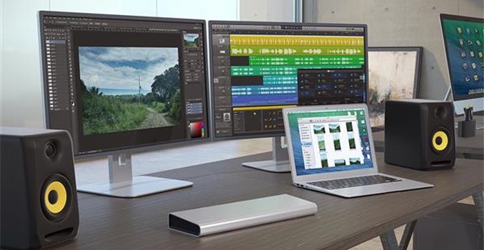
StarTech this week introduced its new docking station for notebooks equipped with Thunderbolt 2 ports, which can hook up to 12 different devices, including displays, storage, audio and LAN, to a single TB2 connector. The device costs $347.99, which is not really affordable, but it offers a comprehensive set of ports that is not available on other docks (at least, according to ThunderboltTechnology.net web-site) and which significantly expands capabilities of any TB2-equipped laptop.

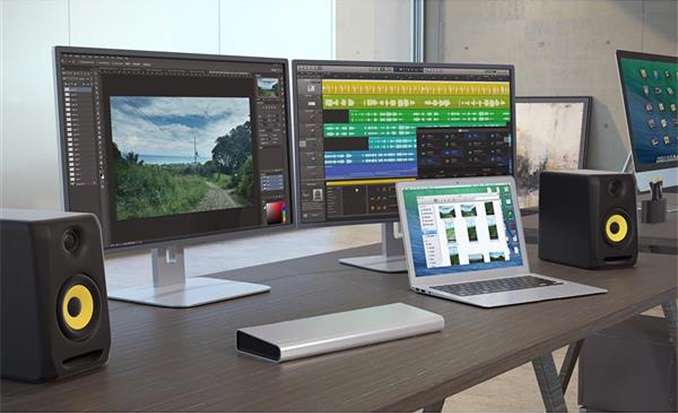
The StarTech Thunderbolt 2 Dual-Monitor Docking Station for Laptops (TB2DOCK4K2DP) is based on the Intel DSL5520 (Falcon Ridge) quad-channel Thunderbolt 2 controller that can transfer data at 20 Gbps while simultaneously driving a single 4K (3840×2160) monitor or two QHD (2560×1440) monitors. The docking station can connect to two displays with up to 3840×2160 and 3440×1440 resolutions using DisplayPort and Thunderbolt connectors (ot just two DisplayPorts), essentially adding dual-monitor capability to any PC with a TB2 connector.

The Thunderbolt 2 Dual-Monitor Docking Station features two Thunderbolt 2 ports, two DisplayPort outputs, four USB 3.0 type-A ports (including one Fast-Charge port) driven by the Fresco Logic FL1100EX controller, one eSATA connector featuring the the ASMedia ASM1061 controller, one Gigabit LAN port enabled by the Intel WGI210AT chip, two 3.5 mm mini-jacks (TI PCM2912A) as well as one SPDIF optical Toslink audio output (CMedia CM6500). From the architectural standpoint, the StarTech Thunderbolt 2 docking station is a huge PCI Express-based expansion module with hot-plug capability. One USB 3.0 port can be used for charging smartphones or other devices compatible with the USB Battery Charging 1.2 specification (delivery of up to 7.5W of power) even when the dock itself is not connected to a PC.

Since the vast majority of Thunderbolt 2-enabled systems are Apple MacBook laptops, the docking station unsurprisingly comes in aluminum casin to match design of Apple’s notebooks. The first MacBook with Thunderbolt 2 was unveiled in late 2013 and by now tens of millions of laptops featuring the interface have been shipped. The existing MacBook user base is also likely why StarTech is releasing a TB2 dock now, even after the recent release of Thunderbolt 3 technology (which offers higher bandwidth and compatibility with USB 3.1). A TB3 dock would be incompatible with the sizable existing base of TB2 users due to the port change (and no adapters are currently available) and meanwhile the number of TB3 systems in the field is still low as adoption of the TB3 by laptop vendors and users is only beginnng.

The 12-port Thunderbolt 2 docking station is available from StarTech today for $347.99. According to StarTech’s press release, the device will also be available from CDW, Amazon.com, Newegg.com, PC Connection, and Insight and will be distributed internationally by Ingram Micro, SYNNEX, Tech Data, D&H and ASI. The package includes the device itself, one copper Thunderbolt cable, one 72W power adapter, four power cords as well as a manual.

Micron 3D NAND Status Update

Micron 3D NAND Status Update

Update: We’ve got some more information and diagrams from Micron’s Winter Analyst Conference earlier today.

After samples of their upcoming 3D NAND were sighted in the wild at CES, Micron has taken the time to provide some details about the flash memory and their plans for it. A lot of this is a recap of information we’ve previously covered, but we’ve got some new details and a better idea of the roadmap for the future.

The entire flash memory industry has shifted focus to the devlopment of 3D NAND flash memory as the replacement for planar NAND flash memory. Samsung took an aggressive approach and has enjoyed some great success with their V-NAND branded 3D NAND, but it hasn’t been an entirely trouble-free transition. Micron has been more conservative both in technology and timing, but they plan on having a strong competitor on the market later this year.

Micron’s first generation 3D NAND takes the form of a 256Gb MLC die and a 384Gb TLC die (compare with their 128Gb 16nm MLC and TLC). At a high level, the die will be partitioned into four separate planes, compared to two planes for most competing NAND. A 480GB drive using the four-plane 256Gb dies will have access to approximately the same amount of parallelism as a 480GB drive using two-plane 128Gb dies, so this capacity jump won’t bring the performance drops that have tarnished some NAND process shrinks.

The key development that allows Micron to produce a four-plane die without inflating die size and cost relative to the two-plane competition is that they’ve layered much of the required additional circuitry under the 3D flash array, instead of sitting alongside. Micron says that their “CMOS Under the Array” design puts more than 75% of the logic (things like address decoding and page buffers) under the flash memory. It doesn’t make the additional segmentation of the four-plane design entirely free, but it allows it to be a very cost effective performance optimization. This is still planar CMOS logic, not any kind of 3D or stacked logic; it’s just got some metal interconnect layers and the flash array piled on top.

On a smaller scale, the 3D NAND will have a page size of 16kB and erase block sizes of 16MB for the MLC and 24MB for the TLC. Because CPUs and filesystems are still mostly dealing with 4kB chunks, Micron has included a partial page read capability that allows for a 4kB read to be done a bit faster and with about half the power of a full 16kB page read. This helps offset some of the penalty the larger page size can have on random 4kB read performance. The large erase block sizes won’t have much of a direct impact on performance and are a necessary efficiency measure: erasing requires charge pumps to produce higher voltages than reads or writes use, and it’s a slower and more power-hungry operation. If you’re going to fire up that extra circuitry and block access to the entire plane for 1ms or more, you might as well erase a usefully large amount of flash.

For the architecture of the individual memory cells, we have nothing new to report. Intel and Micron are alone in their decision to stick with floating-gate flash technology instead of transitioning to charge-trap flash. We’ve previously explained how the technologies differ and what kinds of advantages the manufacturers want to reap from the change. The cost is that the design process involves different tradeoffs that are not as thoroughly explored and understood as the dynamics of floating-gate flash, and for now Micron is sticking with what they know. Micron’s 3D NAND might not have the best write endurance, but they’re expecting to have an advantage in data retention time for healthy flash. They aren’t providing exact numbers, but they’re estimating that drives relying on simpler BCH ECC can get effective program-erase cycle lifetimes in the thousands and drives with LDPC will have effective cycle counts of tens of thousands. Once the process has matured it should exceed their 20nm planar NAND’s write endurance.

The first 3D NAND Micron has ready for the market will produced to the endurance standards for client drives, with enterprise-grade 3D NAND following later. The MLC is currently a few weeks ahead of the TLC in the qualification process, but given the state of the client SSD market the TLC will be the more popular product and will overtake the MLC in volume produced within a few months of 3D NAND drives hitting the market. Overall their 3D NAND will comprise a majority of their flash output on a per-GB basis by the second half of 2016. Micron is sampling drives with 3D NAND to partners this month and is planning for general availability in June. Other drive vendors using Micron’s NAND will be on similar release schedules.

Micron hasn’t announced any specific drive models, but they’ve given a general roadmap that is unsurprising. Consumer and client products will come during the middle of the year, with the capacity and cost improvements allowing for things like 2TB 2.5″ drives and 1TB single-sided M.2 drives. Toward the end of 2016 and into 2017 we’ll see enterprise products such as very high capacity (8TB+) drives and updates in the existing product segments for SAS and PCIe drives.

Looking further to the future, Micron gave a presentation last week at the IEEE International Solid-State Circuits Conference entitled “A 768Gb 3b/cell 3D-Floating-Gate NAND Flash Memory”. This was more about bragging about their R&D in an academic context than announcing any concrete future product plans, but it does represent the most likely successor to their first-generation 3D NAND. The chip in question provides a whopping 768Gb (96GB) capacity when operated as TLC, and 512Gb (64GB) as MLC. The die size is about the same as their 32-layer 384Gb TLC, the areal bit density is almost doubled, and most of the other details are the same—implying that the layer count has probably increased, though Micron isn’t saying how many layers it uses. If Micron has plans to switch to charge-trap flash they’re keeping it under wraps for now, and any such transition isn’t imminent. The second-generation 3D NAND will start production in their Singapore fab this summer, and volume will be ramping up around the end of 2016 (during the second quarter of their fiscal year 2017). Micron predicts their second-generation 3D NAND will be at least 30% cheaper per Gb than the first generation, which they report to be at least 25% cheaper than their 16nm planar NAND.


HP’s New Laptops to Feature AMD FreeSync Technology

HP’s New Laptops to Feature AMD FreeSync Technology

AMD has announced that the new versions HP’s Envy 15z laptops – powered by the company’s latest-generation A-series APUs – will feature the FreeSync variable refresh rate technology. In addition, all of HP’s consumer notebooks powere…

Examining Soft Machines’ Architecture: An Element of VISC to Improving IPC

Last week, Soft Machines announced that their ‘VISC’ architecture was available for licensing, following the announcement of the original concepts over a year ago. The concepts behind their VISC architecture, which splits the workload of a single linear thread across multiple cores in an effort to improve IPC, are intriguing and exciting. But as with any new fundamental change in computer processing, it will be subject to a large barrage of questions. We were invited to a presentation and call with the President and Chief Technical Officer Mohammed Abdallah and the VP Marketing and Business Mark Casey, and I put a number of questions on the lips of analysts to them.

Qualcomm Announces Snapdragon Wear 2100 IoT SoC

Qualcomm Announces Snapdragon Wear 2100 IoT SoC

Along with today’s announcements of the Snapdragon 425, 435 and 625, we also see the reveal of a new wearables-oriented SoC: the Snapdragon Wear 2100. In the past we’ve seen vendors use low-end smartphone SoCs such as the Snapdragon 400 (Motorola Moto 360 2nd gen). In fact, to date only Samsung (Exynos 3250) and Apple (S1) were able to employ chipsets that were specifically designed for wearables. This was rather unfortunate for other wearable vendors as devices such as smartwatches require much higher efficiency and lower power than what “off-the-shelf” SoCs were able to offer. Qualcomm sees to fix this by introducing a new lineup of chips called Snapdragon Wear that are designed with wearables in mind. 

The Snapdragon Wear 2100 is a quad-core Cortex A7 running at up to 800MHz or 1.2GHz (Qualcomm at various points states both) with an Adreno 304 GPU and 400MHz LPDDR3. The choice of using a Cortex A7 is warranted by the fact that Cortex A53s are too power hungry for wearables and that it’s likely too early to see Cortex A35 based SoCs as ARM announced the core only a couple of months ago. A big advantage that Qualcomm has with the Wear 2100 is that it’s able to offer an integrated X5 modem for basic cellular connectivity (Supporting all current standards). 

With the Wear 2100 Qualcomm is now able to offer a fitting SoC for wearable devices and it’s very likely that consumers will see direct benefits such as improved battery life. Qualcomm hasn’t specified any availability for the SoC but discloses that there are multiple devices in development using the processor.